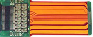
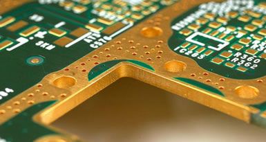
Via is one of the important components of multilayer PCB, and the cost of drilling usually accounts for 30% to 40% of the cost of PCB manufacturing. Simply put, every hole on the PCB can be called a via. From the point of view of function, vias can be divided into two categories: one is used for electrical connections between layers; the other is used for fixing or positioning devices. In terms of process, these vias are generally divided into three categories, namely blind vias, buried vias and through vias. Blind vias are located on the top and bottom surfaces of the printed circuit board and have a certain depth. They are used to connect the surface line and the underlying inner line. The depth of the hole usually does not exceed a certain ratio (aperture).
From a design point of view, a via is mainly composed of two parts, one is the drill hole in the middle, and the other is the pad area around the drill hole. The size of these two parts determines the size of the via. Obviously, in high-speed, high-density PCB design, designers always hope that the smaller the via hole is, the better, so that more wiring space can be left on the board. In addition, the smaller the via hole, the parasitic capacitance of its own. The smaller it is, the more suitable it is for high-speed circuits. However, the reduction of hole size also brings about an increase in cost, and the size of vias cannot be reduced indefinitely. It is limited by process technologies such as drilling and plating: the smaller the hole, the more drilling The longer the hole takes, the easier it is to deviate from the center position; and when the depth of the hole exceeds 6 times the diameter of the drilled hole, it cannot be guaranteed that the hole wall can be uniformly plated with copper. For example, if a normal 6-layer PCB board has a thickness (through hole depth) of 50Mil.

Then, under normal conditions, the smallest hole diameter that PCB manufacturers can provide can only reach 8Mil. With the development of laser drilling technology, the size of the hole can be smaller and smaller. Generally, a via with a diameter less than or equal to 6Mils is called a microhole. Microvias are often used in HDI (High Density Interconnect Structure) designs. Microvia technology allows vias to be directly punched on the pad (Via-in-pad), which greatly improves circuit performance and saves wiring space.
Parasitic capacitance and inductance of vias
The via itself has parasitic stray capacitance. If it is known that the diameter of the solder mask on the ground layer of the via is D2, the diameter of the via pad is D1, the thickness of the PCB board is T, and the dielectric constant of the board substrate Is ε, then the parasitic capacitance of the via is similar to:
C=1.41εTD1/(D2-D1)
The main effect of the parasitic capacitance of the via on the circuit is to extend the rise time of the signal and reduce the speed of the circuit. For example, for a PCB with a thickness of 50Mil, if the diameter of the via pad used is 20Mil (the diameter of the hole is 10Mils), and the diameter of the solder mask is 40Mil, then we can approximate the size of the via using the above formula The parasitic capacitance is roughly:
C=1.41x4.4x0.050x0.020/(0.040-0.020)=0.31pF
The amount of change in rise time caused by this part of the capacitance is roughly:
T10-90=2.2C(Z0/2)=2.2x0.31x(50/2)=17.05ps
From these values, it can be seen that although the effect of the rise delay caused by the parasitic capacitance of a single via is not very obvious, if the via is used multiple times in the trace to switch between layers, multiple vias will be used., The design must be carefully considered. In actual design, the parasitic capacitance can be reduced by increasing the distance between the via hole and the copper area (Anti-pad) or reducing the diameter of the pad.
How to use vias
Through the above analysis of the parasitic characteristics of vias, we can see that in high-speed PCB design, seemingly simple vias often bring great negative effects to circuit design. In order to reduce the adverse effects caused by the parasitic effects of the vias, the following can be done in the design:
A Considering both cost and signal quality, choose a reasonable size via size. If necessary, you can consider using different sizes of vias. For example, for power or ground vias, you can consider using a larger size to reduce impedance, and for signal traces, you can use smaller vias. Of course, as the size of the via decreases, the corresponding cost will increase.
B The two formulas discussed above can be drawn, using a thinner PCB is beneficial to reduce the two parasitic parameters of the via.
C. The signal traces on the PCB board should not be changed as much as possible, which means that unnecessary vias should not be used as much as possible.
D The pins of the power supply and the ground should be drilled nearby, and the lead between the via and the pin should be as short as possible. Consider drilling multiple vias in parallel to reduce the equivalent inductance.
E Place some grounded vias near the vias of the signal change layer to provide the closest return to the signal. You can even place some redundant ground vias on the PCB.
F For high-density high-speed PCB boards, you can consider using micro vias.