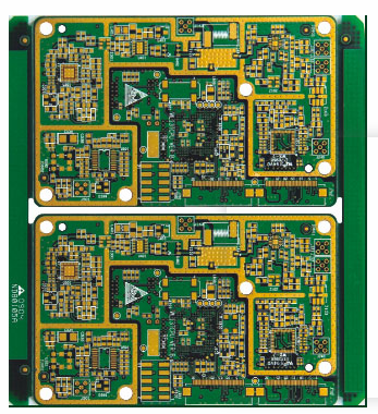
What is PCB board film
Film is film, which is the old translation of film. Now it generally refers to film, and it can also refer to the negatives in printing. The film introduced in this article refers to the negatives in the printed circuit board.

Films are all black, and the film number is an English symbol. On the corner of the film, indicate which of the C, M, Y, or K the film is, and it is one of the cmyk (or spot color numbers). Indicates the color of the film output. If not, you can look at the angle of the screen to identify the color. The stepped color bar next to it is used for dot density calibration.
The color bar is not only to see if the dot density is normal, but also to look at CMYK, which is generally judged by the position of the color bar: the color bar is C in the lower left corner, the color bar is M in the upper left corner, and Y is in the upper right corner. The lower right corner is K, so as long as the printing factory knows CMYK according to the color bar. That is to say, in order to facilitate the inspection of the concentration of the film development, there are color numbers on the corners of the film. As for the number of colors to be printed, it is determined by the screen line of each film.
The main composition of film film is protective film, emulsion layer, bonding film, film base and anti-halation layer. The main components are silver salt photosensitive material, gelatin and pigment. Silver salt can reduce the silver core center under the action of light, but it is not dissolved in water. Therefore, gelatin can be used to make it into a suspended state and coated on the film base. The emulsion also contains pigments for sensitization. Then the exposure film is obtained through actinic action.
Circuit board film flushing process
The film can be processed after exposure. Different negatives have different processing conditions. Before use, you should read the instructions for use of the negatives carefully to determine the correct developer and fixer formulations.
The process of film processing is as follows:
Exposure imaging: that is, after the film is exposed, the silver salt restores the silver center, but at this time, no graphics can be seen on the film, which is called a latent image.
Development:
is about to reduce the silver salt after irradiation into black silver particles. During manual development, the exposed silver salt film is evenly immersed in the developer solution. Since the silver salt film used in the production of printed boards has a low photosensitive speed, the development process can be monitored under a safety light, but the light should not be too bright, To avoid running out of negative film. When the black images on the front and back of the negative have the same color depth, the development should stop.
Take the film out of the developing solution, rinse it with water or acid stop solution, then put it into the fixing solution and fix it. The temperature of the developer has a great influence on the development speed. The higher the temperature, the faster the development speed. The suitable developing temperature is 18~25OC.
The machine developing process is automatically completed by the automatic filming machine, pay attention to the concentration ratio of the medicine. Normally, the concentration ratio of the developing solution for machine punching is 1:4, that is, the developing solution of 1 measuring cup volume is evenly blended with 4 measuring cups of clean water.
Fixing:
is to dissolve the silver salt that has not been reduced to silver on the negative to prevent this part of the silver salt from affecting the negative image after exposure. The time for manual film-finishing and fixing is doubled after no photosensitive parts on the film are transparent. The filming and fixing process of the machine is also automatically completed by the automatic filming machine. The concentration ratio of the medicine can be slightly thicker than that of the developing medicine.
Washing:
The fixed film is stuck with chemicals such as sodium thiosulfate. If it is not rinsed, the film will turn yellow and become invalid. Hand-punched tablets are usually rinsed with running water for 15-20 minutes. The washing and drying process of the machine's film processing is automatically completed by the automatic film processing machine.
air dry:
The hand-finished negatives should also be stored in a cool and dry place after air-drying.
In the above process, be careful not to scratch the film, and at the same time, do not splash chemical solutions such as developing and fixing liquid on the human body and clothing.
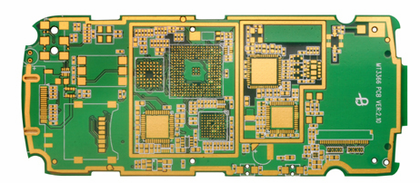
The PCB board design and production process has as many as 20 processes. Poor tinning is really a headache. Poor tin on the PCB board may cause such as circuit sand holes, chipping, circuit dog teeth, open circuit, and circuit sand holes. Wire; if the hole is too thin, there will be no copper; if the tin is not cleaned (the number of times the tin is returned will affect the uncleanness of the plating layer) and other quality problems, so encountering poor tin often means re-soldering or even abandonment of previous efforts, Needs to be remade.

What are the reasons for poor tin on PCB boards
The PCB board may not be well tinned during SMT production. Generally, the poor tinning is related to the cleanliness of the bare PCB board surface. If there is no dirt, there will be basically no poor tinning. Poor flux, temperature, etc. when tinning.