Nowadays, the long-life laser source configured in the laser system is basically close to being maintenance-free. In the production process, the laser level is level 1, and no other protective devices are required for safety. The LPKF laser system is equipped with a dust collection device, which will not cause the emission of harmful substances. Coupled with its intuitive and easy-to-operate software control, laser technology is replacing traditional mechanical processes, saving the cost of special tools.
For example, when PCB splitting or cutting, you can choose a CO2 laser system with a wavelength of about 10.6μm. The processing cost is relatively low, and the laser power provided can reach several kilowatts. But it will generate a lot of heat energy during the cutting process, which will cause severe carbonization of the edges.
The wavelength of the UV laser is 355 nm. Laser beams of this wavelength are very easy to focus optically. The spot diameter of a UV laser with a laser power of less than 20 watts is only 20μm after focusing-and the energy density it generates is even comparable to that of the sun's surface.
UV laser is especially suitable for cutting and marking hard boards, rigid-flex boards, flexible boards and their accessories. So what are the advantages of this laser process?
In the fields of circuit board sub-boarding in the SMT industry and micro-drilling in the PCB industry, the UV laser cutting system shows great technical advantages. Depending on the thickness of the circuit board material, the laser cuts one or more times along the required contour. The thinner the material, the faster the cutting speed. If the accumulated laser pulse is lower than the laser pulse required to penetrate the material, only scratches will appear on the surface of the material; therefore, two-dimensional code or barcode marking can be performed on the material for information tracking in subsequent processes.

The pulse energy of the UV laser only acts on the material for a microsecond level, and there is no obvious thermal effect at a few micrometers next to the cut, so there is no need to consider the damage to the components caused by the heat generated. The lines and solder joints near the edge are intact and free of burrs.
In addition, the LPKF UV laser system integrated CAM software can directly import the data exported from CAD, edit the laser cutting path, form the laser cutting contour, select the processing parameter library suitable for different materials, and then directly laser processing. The laser system is not only suitable for mass production processing, but also for sample production.
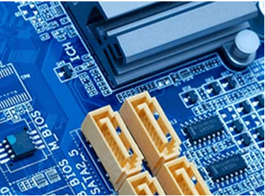
The through holes in the circuit board are used to connect the lines between the front and back of the double-sided board, or to connect any interlayer lines in the multilayer board. In order to conduct electricity, the wall of the hole needs to be plated with a metal layer after drilling. Nowadays, traditional mechanical methods can no longer meet the requirements of smaller and smaller drilling diameters: although the spindle speed is increased, the radial speed of precision drilling tools will be reduced due to the small diameter, and even the required processing results cannot be achieved. In addition, from an economic perspective, tool consumables that are prone to wear are also a limiting factor.
For the drilling of flexible circuit boards, when drilling, the laser can firstly cut out the micro-hole outline from the center of the hole, which is more accurate than ordinary methods. The system can drill micro-holes with a minimum diameter of 20μm on organic or non-organic substrates under the condition of high-diameter-depth ratio. Flexible circuit boards, IC substrates or HDI circuit boards all require such precision.
In the manufacturing process of electronic components, what situations require cutting of prepreg material? In the early days, prepreg materials have been used in multilayer circuit boards. The various circuit layers in the multi-layer circuit board are pressed together by the action of the prepreg; according to the circuit design, the prepreg in some areas needs to be cut and opened in advance and then pressed.
A precise contour can be formed on the sensitive cover layer by laser processing.
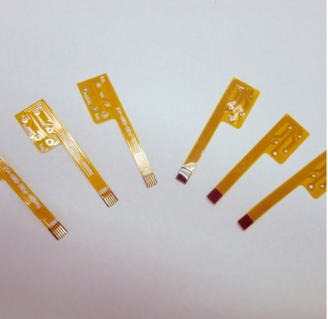
A similar process is also applicable to FPC cover film. The cover film is usually composed of polyimide and a glue layer with a thickness of 25 μm or 12.5 μm, and is easily deformed. A single area (such as a pad) does not need to be covered by a cover film for later assembly and connection work.
This thin material is very sensitive to mechanical stress-it can be easily done by non-contact laser processing. At the same time, the vacuum suction table can well fix its position and maintain its flatness.
In the rigid-flex board, the rigid PCB and the flexible PCB are pressed together to form a multilayer board. During the pressing process, the upper part of the flexible PCB is not pressed and bonded to the rigid PCB. The rigid cover covering the flexible PCB is cut and separated by laser depth cutting, leaving the flexible part to form a rigid-flex board.
Such fixed-depth processing is also suitable for the blind groove processing of embedded integrated components on the surface of the multilayer board. The UV laser will accurately cut the blind grooves of the target layer separated from the multilayer circuit board. In this area, the target layer cannot form a connection with the material covered on it.
After SMT, the sub-board is to cut the circuit board on which a variety of electronic components have been assembled. This process is already at the end of the production chain. For board splitting, different technologies can be selected: For commonly used PCBs, priority is given to the use of traditional cutting, stamping and contour milling processes. For more complex electronic circuits and thin substrates, especially those that are very sensitive to mechanical stress, dust, and dimensional deviation, it is more advantageous to use UV laser cutting to separate the board. The following three charts evaluate these three methods from different factors.
Due to the short wavelength of UV laser, it is suitable for most material processing. For example, it can be used in the electronics industry:
Not limited to the processing of circuit boards, the UV laser system can also complete the cutting, direct writing and drilling of LTCC components in one processing operation.
For laser cutting or drilling in the circuit board industry, only a few watts or more than ten watts of UV laser are required, and no kilowatt-level laser power is required. In consumer electronics, automotive industry or robot manufacturing technology, flexible circuit boards are Use becomes increasingly important. Because the UV laser processing system has flexible processing methods, high-precision processing effects and flexible and controllable processing, it has become the first choice for laser drilling and cutting of flexible circuit board s and thin PCBs.