5G brings new design and manufacturing challenges to high frequency. To meet 5G technical requirements, strict pattern designs and complex materials are required. Therefore, the industry needs to adopt new imaging, inspection and measurement technologies to manufacture PCB s required for 5G infrastructure and equipment.
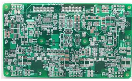
5G infrastructure such as cellular base stations, data servers, high-performance computing systems, and artificial intelligence have increased the demand for fine-line IC carrier boards and high-level digital (HLC) multi-layer boards (MLB). In terms of equipment, 5G antennas, camera modules, and display drivers have increased the demand for high-density interconnection (HDI) at any layer, and higher-density PCBs with advanced HDI. All these 5G-oriented PCB design requirements push or exceed the limits of traditional technologies.
Imaging technology
Some advanced manufacturing technologies are expected to provide the imaging and inspection capabilities required to manufacture higher quality and more complex PCBs to meet 5G technical requirements. These include direct imaging (DI), automatic optical inspection (AOI), and automatic optical shaping and repair. However, the manufacturing requirements for PCBs used in 5G infrastructure and 5G equipment are not the same.
As far as 5G infrastructure is concerned, DI technology can achieve the strict impedance control required for high-frequency 5G (such as millimeter waves), as well as high precision and strict upper and lower layer alignment accuracy on large panels, thereby meeting the requirements for high-level digital MLB . The high-capacity solder mask (SM) DI technology can support large size (up to 32 inches) and warped panels, while meeting the 5G requirements for higher resolution and accuracy.
Automatic optical inspection
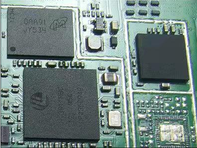
Ideally, Automated Optical Inspection (AOI) should provide inspection and measurement with almost no manual processing, and have the ability to detect fine lines of IC carrier boards as small as 5 μm, which is a typical feature of HPC and data servers in 5G infrastructure .
For 5G devices, DI can provide high-quality imaging to meet the requirements of improved semi-additive process (mSAP) or carrier-like PCB (SLP) production processes for fine lines, precise conductor geometries, high precision, and advanced scaling. At the same time maintain the highest effective production capacity and yield. With the growing demand for smaller form factors, lighter weights, and more advanced features in 5G electronic products, the importance of flexible printed circuit (FPC) components is increasing, bringing new challenges to manufacturing. The roll-to-roll DI system enables FPC manufacturers to use roll-based flexible materials while maintaining their integrity and minimizing frequent damage and deformation.
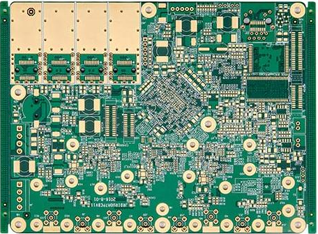
The PCB AOI used in the device can be integrated with 2D laser blind hole measurement to measure the size of the blind hole, including the top and bottom diameter, roundness and taper, and position. In addition, AOI integrated with automatic 2D linewidth measurement (Figure 1) is the key to ensuring accurate top and bottom measurements to achieve impedance control, and it is also critical for components such as 5G millimeter wave antenna boards.
Generally speaking, 5G PCB inspection needs must address challenges such as low-contrast material layers, transparent flexible printed circuits, laser blind hole inspection, fast and accurate measurements for impedance control, and low cost of ownership. Some inspection processes can also perform high-contrast imaging on low-contrast materials, so as to achieve complete detection without false alarms.
There is another innovative process worth considering: automatic optical shaping and repairing. With this type of optical repair technology, manufacturers can shape open and short circuits at high speed and high quality when identifying advanced HDI (mSAP) PCBs and IC carrier boards in the production line. This technology greatly reduces the scrap of plates and panels, saves time and manpower by eliminating manual repair links, and improves overall quality and production yield. With the help of advanced automatic optical repair technology, manufacturers can increase the yield and quality in the mass production of 5G PCBs, thereby enhancing their competitive advantage.
Design and manufacture
Challenge 5G's influence on PCB and IC carrier board design and process can achieve more accurate mass production.