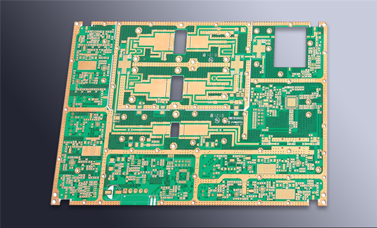
1. Draw the wiring area within 1mm from the edge of the PCB board and within 1mm around the mounting hole, and wiring is forbidden.
2. The power line should be as wide as possible and should not be less than 18mil; the signal line width should not be less than 12mil; the cpu input and output lines should not be less than 10mil (or 8mil); the line spacing should not be less than 10mil.
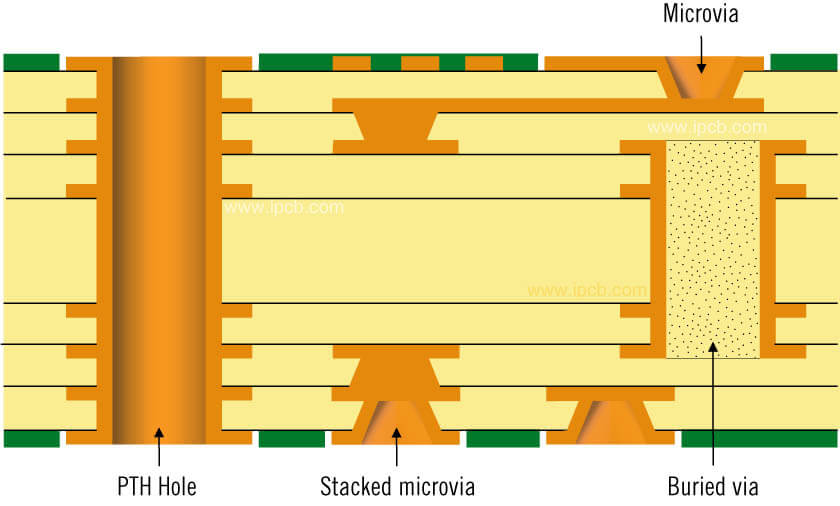
3. The normal via is not less than 30mil.
4. Note that the power line and the ground line should be as radial as possible, and the signal line must not be looped.
5. Ground circuit rules:
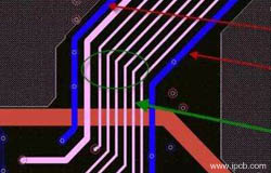
The minimum loop rule is that the loop area formed by the signal line and its loop should be as small as possible. The smaller the loop area, the less the external radiation and the less interference from the outside world. An example is shown in the figure below:

6. Crosstalk control
Crosstalk refers to the mutual interference between different networks on the PCB due to long parallel wiring, mainly due to the distributed capacitance and distributed inductance between the parallel wires. The main measures to overcome crosstalk are:
Increase the spacing of parallel wiring and follow the 3W rule.
Insert a grounded isolation wire between the parallel wires. Reduce the distance between the wiring layer and the ground plane.
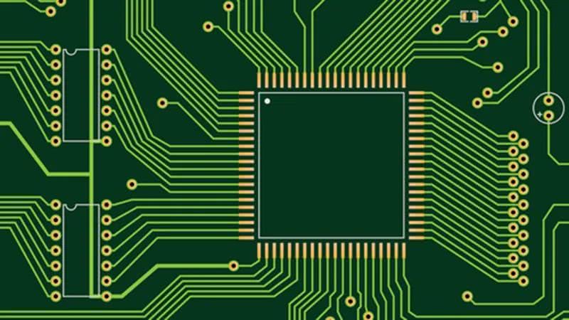
7. Direction control rules for routing:
The routing directions of adjacent layers are orthogonal. Avoid running different signal lines in the same direction on adjacent layers to reduce unnecessary inter-layer crosstalk; when this situation has been avoided due to board structure limitations, especially when the signal rate is high, you should consider using a ground plane to isolate each Wiring layer, isolate each signal line with ground signal line. The printed wires of the PCB circuit board used as the input and output of the circuit should be avoided as far as possible to avoid parallelism, so as to avoid feedback. It is best to add a grounding wire between these wires.
8. Open-loop inspection rules for wiring:
Generally, it is not allowed to have a floating wiring at one end, mainly to avoid the "antenna effect" and reduce unnecessary interference radiation and reception, otherwise it may bring unpredictable results.
9. Impedance matching inspection rules:
The wiring width of the same network should be kept consistent. Variations in line width will cause uneven line characteristic impedance, and reflections will occur when the transmission speed is high. This situation should be avoided as much as possible in the design. Under certain conditions, such as the similar structure of the lead wire of the connector and the lead wire of the BGA package, the change of the line width may not be avoided, and the effective length of the middle inconsistent part should be minimized.
10. Closed-loop wiring inspection rules:
Prevent signal lines from forming self-loops between different layers. Such problems are prone to occur in multi-layer PCB design, and self-loop will cause radiation interference.
11. The branch length control rules of the wiring:
Try to control the length of branches, the general requirement is Tdelay "=Trise/20.
12. Resonance rules of wiring:
Mainly for high-frequency signal design, that is, the length of the wiring must not be an integer multiple of its wavelength to avoid resonance.
13. Line length control rules:
That is to say, the short-line rule. In PCB design, the wiring length should be kept as short as possible to reduce interference problems caused by excessively long wiring. Especially for some important signal lines, such as clock lines, be sure to place their oscillators very far away from the device. Near place. In the case of driving multiple devices, the network topology should be decided according to the specific situation.