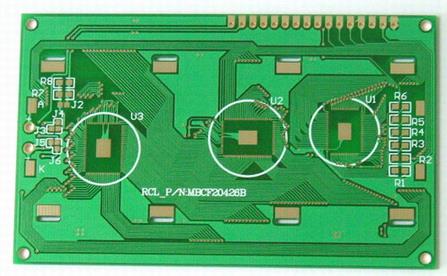
Printed circuit boards are the supporting parts of circuit components and devices in electronic products. It provides electrical connections between circuit components and devices and is the most basic component of various electronic devices. At present, large and very large scale integrated circuits have been widely used in electronic equipment, and the mounting density of components on the printed circuit board is increasing, and the signal transmission speed is getting faster and faster. The EMC problems caused by this are also becoming increasingly prominent. . Printed circuit boards are divided into single-sided boards (single-layer boards), double boards (double-layer boards) and multilayer boards. Single and dual boards are usually used for low and medium density wiring and low integration circuits, while PCB multilayer boards use high density wiring and high integration circuits. Single and double boards are not suitable for high-speed circuits, and single and double-sided wiring cannot meet the requirements of high-performance circuits. The development of multilayer wiring technology provides the possibility to solve the above problems, and its applications are becoming increasingly widespread.
Features of multilayer wiring.
The circuit board is composed of organic and inorganic dielectric materials and has a multi-layer structure. The layers are connected by vias. Via plating or filling metal materials can realize the electrical signal conduction between the layers. Due to the following characteristics, multilayer wiring has been widely used:
A dedicated power supply layer and a ground wire layer are provided in the multi-layer board. The power layer can be used as a noise source to reduce interference; at the same time, the power layer can provide a loop for all signals of the system to eliminate common impedance coupling interference. Reduce the impedance of the power supply line in the power supply system, thereby reducing the common impedance interference.
(2) Multilayer boards use a special ground layer, and all signal lines have special ground wires. The characteristics of the signal line: stable impedance, good matching, reduce waveform distortion caused by reflection; use a special ground layer, increase the distributed capacitance between the signal line and the ground line, and reduce crosstalk.
Third, the laminated design of the printed circuit board.
Wiring rules of the PCB board.

The electromagnetic compatibility analysis of the multilayer board can be carried out according to Kirchhoff's law and Faraday's law. According to Kirchhoff's law, any time-domain transmission signal from the signal source to the load must have the lowest impedance path.
PCBs with multi-layer boards are usually used in high-speed and high-performance systems, where multi-layer boards can be used for direct current (DC) power or ground reference planes. Since there are enough layers as power or ground layers, these planes are usually not divided into solid planes, so it is not necessary to place different DC voltages in the same layer. This layer will serve as a current loop back to the signal on the adjacent transmission line. Building a low-impedance current loop is the primary goal of this type of planar layer EMC.
The signal layers are distributed between the physical layers of the reference plane, and they can be symmetrical striplines or asymmetrical striplines. The structure and layout of the multi-layer board are described with a 12-layer board as an example. Its hierarchical structure is T-P-S-P-S-P-B, where T is the uppermost layer, P is the reference plane, S is the signal layer, and B is the lowermost layer. From top to bottom, there are 1 layer, 2 layers, ..., 12 layers. As the upper and lower pads of the component, the signal cannot be transmitted over a long distance between the upper and the lower, which can reduce the direct radiation of the trace. Incompatible signal lines should be isolated from each other, the purpose of which is to avoid coupling interference between each other. High frequency and low frequency, high current and small current, digital and analog signal lines are incompatible. Incompatible components should be placed in different positions on the printed board for component layout, and attention should be paid to isolating signal lines when arranging them . Three issues should be paid attention to in the design:
Decide which reference layer will contain multiple power regions for different DC voltages. Assuming that the eleventh layer has multiple DC voltages, the designer must keep the high-speed signals as far away as possible from the tenth layer and the bottom layer, because the loop current cannot pass through the reference plane above the tenth layer, and stitch capacitors need to be used; third, The fifth, seventh and ninth layers are the signal layers for high-speed signals. The routing of key signals should be arranged in one direction as much as possible, so that the number of possible routing channels can be determined on the optimization layer. The signal traces between the layers should be perpendicular to each other, which can reduce the coupling interference between the electric field and the magnetic field. The third and seventh layers can be set up with "east-west" wiring, and the fifth and ninth layers can be set with "south-north" wiring. Which layer of fabric should be based on the direction it reaches the destination
(2) The change in the number of layers during high-speed signal routing and which layer is used in an independent routing to ensure that the return current flows from a reference plane to the required new reference plane. This is to reduce the area of the signal loop and reduce the loop differential-mode current radiation and common-mode current radiation. The radiation intensity of the loop is proportional to the area of the loop. In fact, the best design does not need to change the reference surface, only one side of the reference surface needs to be changed, and only need to be changed back to the other side. For example, a combination of signal layers can be used as signal layer pairs: Nos. 3, 5, 7, 7, and 9, so that wiring combinations can be formed in the east-west and north-south directions. But the combination of the third and ninth layers cannot be used because it requires the return current to flow from the fourth layer to the eighth layer. Although the decoupling capacitor can be placed near the via, it will lose its function at high frequencies due to the presence of the lead and via inductance. However, such traces will increase the area of the signal loop, and disadvantageously reduce current radiation.
(3) Select the DC voltage of the reference layer. In this case, due to the faster internal signal processing speed of the processor, a lot of noise is generated on the power/ground reference pin. Therefore, it is important to use decoupling capacitors when providing the same DC voltage to the processor and using decoupling capacitors as efficiently as possible. The best way to reduce the inductance of these components is to connect the traces as short as possible, as wide as possible, and the vias as short as possible and too thick.
When the second layer is assigned as "ground" and the fourth layer is assigned as the processor's power supply, the farther the via distance is, the shorter the top layer of the processor and the decoupling capacitor should be. There is no important current in the space extending to the bottom of the board, and there is no antenna function when short-circuited. The reference configuration of the cascading design layout is listed in Table 1.
20-H rule, 3-W rule.
There are two basic principles to determine the distance between the power supply layer of the multilayer board capacitor and the edge of the board in the capacitor design of the multilayer PCB board, and to solve the distance between the printed strips: 20-H method and 3-W method.
20-H principle: RF current usually exists at the edge of the power plane. This is because of the connection between magnetic fluxes. When high-speed digital logic and clock signals are used, the RF currents are coupled with each other, as shown in Figure 1. In order to reduce this effect, the physical size of the power plane should be at least 20H smaller than the physical size closest to the ground plane (H is the distance between the power plane and the ground plane). The edge effect of the power plane generally occurs at about 10H, and at 20H, About 10% of the magnetic flux is blocked, if you want to reach 98% of the magnetic flux, a 100% boundary value is required, as shown in Figure 1. The 20-H rule determines the physical distance between the power plane and the nearest ground plane including the thickness of the copper clad laminate, pre-filling and insulating isolation layer. Using 20-H can increase the resonant frequency of the PCB.
3-W rule: When the distance between two PCB printed lines is small, electromagnetic crosstalk will be generated, which will affect the normal operation of related circuits. In order to avoid this interference, the distance between printed lines should be no less than 3 times, that is, no less than 3W (W is the width of the printing line). The printed line width is related to the line impedance requirements. Too wide affects the wiring density, too narrow affects signal integrity, and too narrow affects the strength of the transmission terminal. The basic application objects of the 3-W principle are clock circuits, differential pairs and I/O port wiring. The "3-W principle" simply points out the electromagnetic flux boundary at which crosstalk energy attenuates by 70%. If higher requirements are required, for example, the electromagnetic flux boundary at which crosstalk energy attenuation is guaranteed to be attenuated by 98% must be 10.