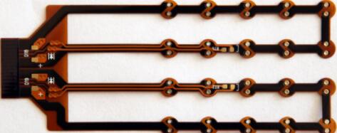
Circuit boards are divided into rigid circuit boards, flexible circuit boards, and rigid-flex boards. The general PCB is called a rigid (Rigid) PCB. The intuitive difference between a rigid PCB and a flexible PCB is that the flexible PCB can be bent. The common thicknesses of rigid PCBs are 0.2mm, 0.4mm, 0.6mm, 0.8mm, 1.0mm, 1.2mm, 1.6mm, 2.0mm, etc. The common thickness of flexible PCB is 0.2mm, and the parts to be welded will have a thickened layer behind it. The thickness of the thickened layer varies from 0.2mm to 0.4mm. The purpose of understanding these is to provide structural engineers with a spatial reference when designing. Common materials for rigid PCB include: phenolic paper laminate, epoxy paper laminate, polyester glass mat laminate, epoxy glass cloth laminate; common materials for flexible PCB include: polyester film, polyimide Amine film, fluorinated ethylene propylene film.
Classification according to the number of circuit layers: divided into single-sided, double-sided and multi-layer boards. Common multi-layer boards are generally 4-layer boards or 6-layer boards, and complex multi-layer boards can reach dozens of layers.
Single panel
Single-Sided Boards On the basic PCB, the parts are concentrated on one side, and the wires are concentrated on the other side (when there are SMD components and the wires are on the same side, the plug-in device is on the other side). Because the wires only appear on one side, this kind of PCB is called a single-sided (Single-sided). Because single-sided boards have many strict restrictions on the design of the circuit (because there is only one side, the wiring cannot cross and must be around a separate path), so only early circuits use this type of board.
Double panel

PCB Double-Sided Board This type of circuit board has wiring on both sides, but to use wires on both sides, there must be a proper circuit connection between the two sides. The "bridge" between such circuits is called a via. A via is a small hole filled or coated with metal on the PCB, which can be connected with the wires on both sides. Because the area of the double-sided board is twice as large as that of the single-sided board, the double-sided board solves the difficulty of interlacing wiring in the single-sided board (it can be conducted to the other side through holes), and it is more suitable for use in circuits that are more complicated than the single-sided board.
Multilayer board
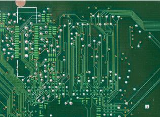
Multi-Layer Boards In order to increase the area that can be wired, multi-layer boards use more single or double-sided wiring boards. Use one double-sided as the inner layer, two single-sided as the outer layer, or two double-sided as the inner layer and two single-sided as the outer layer of the printed circuit board. The positioning system and the insulating bonding material alternately together and the conductive pattern Printed circuit boards that are interconnected according to design requirements become four-layer and six-layer printed circuit boards, also known as multilayer printed circuit boards. The number of layers of the board does not mean that there are several independent wiring layers. In special cases, empty layers are added to control the thickness of the board. Usually, the number of layers is even and includes the outer two layers. Most motherboards have 4 to 8 layers of structure, but technically it can be a PCB board of nearly 100 layers. Most large supercomputers use fairly multi-layered motherboards, but because these types of computers can already be replaced by clusters of many ordinary computers, super-multilayered boards have gradually ceased to be used. Because the various layers in the PCB are tightly integrated, it is generally not easy to see the actual number, but if you look closely at the motherboard, you can still see it.
Features
The reason why PCB can be used more and more widely is that it has many unique advantages, which are summarized as follows.
High density PCB. For decades, the high density of printed boards has been able to develop along with the improvement of integrated circuit integration and the advancement of mounting technology.
High reliability. Through a series of inspections, tests and aging tests, the PCB can work reliably for a long time (usually 20 years).
Designability. For PCB performance (electrical, physical, chemical, mechanical, etc.) requirements, printed board design can be achieved through design standardization, standardization, etc., with short time and high efficiency.
Manufacturability. With modern management, standardized, scaled (quantitative), automated and other production can be carried out to ensure product quality consistency.
Testability. A relatively complete test method, test standard, various test equipment and instruments have been established to detect and appraise the eligibility and service life of PCB products.
Can be assembled. PCB products are not only convenient for standardized assembly of various components, but also for automated and large-scale mass production. At the same time, PCB and various component assembly parts can be assembled to form larger parts and systems, up to the complete machine.
Maintainability. Since PCB products and various component assembly parts are designed and produced on a large scale, these parts are also standardized. Therefore, once the system fails, it can be replaced quickly, conveniently and flexibly, and the system can be quickly restored to work. Of course, there can be more examples. Such as miniaturization and weight reduction of the system, and high-speed signal transmission.