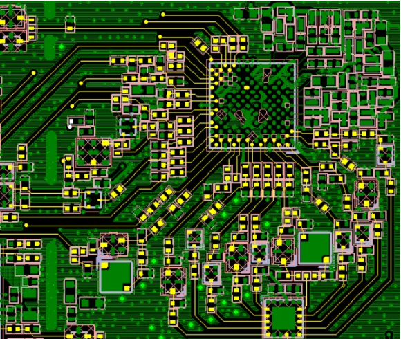
Why should copper be laid? There are generally several reasons for copper laying.
1. EMC. For large-area ground or power supply copper, it will play a shielding role, and some special grounds, such as PGND, play a protective role.
2. PCB process requirements. Generally, in order to ensure the effect of electroplating or the lamination is not deformed, copper is laid on the PCB layers with less wiring.
3. The signal integrity is required to provide a complete return path for high-frequency digital signals and reduce the wiring of the DC network.
Of course, there are heat dissipation, special device installation requires copper and other reasons.

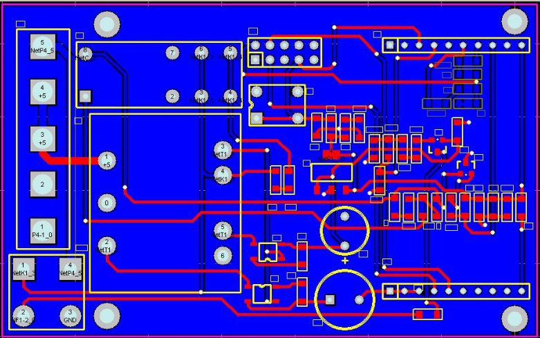
One. One of the major benefits of copper paving is to reduce the ground wire impedance (a large part of the so-called anti-interference is also caused by the reduction of ground wire impedance). There are a lot of spike currents in digital circuits, so it is more necessary to reduce the ground wire impedance. It is generally believed that a large area of ground should be laid for circuits composed of digital devices, while for analog circuits, the ground loop formed by laying copper will cause electromagnetic coupling interference to outweigh the gains (except for high-frequency circuits). Therefore, it is not that all circuits require ordinary copper (BTW: the performance of mesh copper paving is better than that of a whole block)
2. The significance of circuit copper laying lies in:
1. Pave copper and connect with the ground wire, which can reduce the loop area
2. A large area of copper is equivalent to reducing the resistance of the ground wire and reducing the voltage drop. The digital ground and the analog ground should also be separated to lay the copper when the frequency is high, and then connected with a single point. The single point can be connected with a wire around a magnetic ring several times. However, if the frequency is not too high, or the working conditions of the instrument are not bad, it can be relatively relaxed. The crystal oscillator can be regarded as a high-frequency emission source in the circuit. You can spread copper around and ground the shell of the crystal oscillator, which will be better.
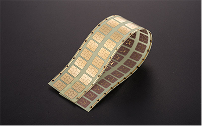
The classification of FPC circuit boards is classified according to its medium and structure, and is organized as follows:
1. Single-layer soft board structure FPC circuit board
The flexible board with this structure is the simplest flexible board. This is usually the base material + transparent glue + copper foil is a set of purchased raw materials, of course the protective film + transparent glue is another purchased raw material. First of all, the material copper foil needs to be processed by etching and other processes to obtain the required circuit, and to reach the protective film, it needs to be drilled to expose the corresponding pads. After cleaning, use the rolling method to combine the two. Then the exposed pad part is electroplated with gold or tin for protection. In this way, the slab is ready. Generally, small circuit boards of corresponding shapes are also stamped. There are also solder masks directly printed on the copper foil without a protective film, so the cost will be lower, but the mechanical strength of the circuit board will be worse. Unless the strength requirements are not high but the price needs to be as low as possible, it is best to apply a protective film method.
2. Double-layer soft board structure
The structure of the FPC double-layer soft board: When the circuit is too complicated, the single-layer board cannot be wired or copper foil is required for grounding shielding, it is necessary to use a double-layer board or even a multilayer board. The most typical difference between a multi-layer board and a single-layer board is the addition of a via structure to connect each layer of copper foil. The first processing technology of general substrate + transparent glue + copper foil is to make vias. First drill holes on the substrate and copper foil, and then plate a certain thickness of copper after cleaning, and the vias are completed. The subsequent production process is almost the same as the single-layer board.
3. Double-sided soft board structure
The structure of the FPC double-sided soft board: There are pads on both sides of the double-sided board, which are mainly used for connection with other circuit boards. Although it is similar to the single-layer board structure, the manufacturing process is very different. Its raw material is copper foil, protective film + transparent glue. Firstly, drill holes on the protective film according to the requirements of the pad position, and then paste the copper foil to corrode the pads and leads, and then paste another drilled protective film.