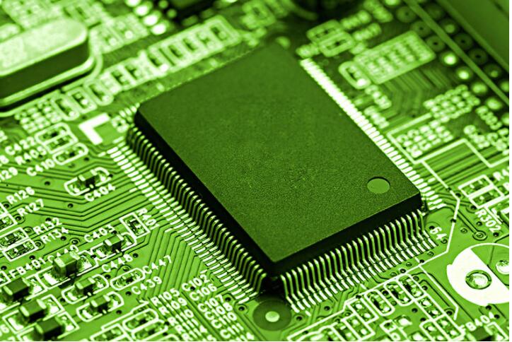
The printed circuit board is mainly composed of pads, vias, mounting holes, wires, components, connectors, filling, electrical boundaries, etc. The main functions of each component are as follows:
1. Pad: A metal hole used to weld the pins of components.
2. Via: A metal hole used to connect the pins of components between layers.
3. Mounting hole: used to fix the printed circuit board.
4. Wire: Copper film used to connect the electrical network of component pins.
5. Connectors: components used to connect between circuit boards.

6. Filling: It is used for the copper coating of the ground wire network, which can effectively reduce the impedance.
7. Electrical boundary: used to determine the size of the PCB circuit board, all components on the circuit board cannot exceed the boundary
PCB special components refer to the key components of the high-frequency part, the core components in the circuit, the components that are susceptible to interference, the components with high voltage, the components with large heat generation, and some components of the opposite sex. These special The location of the components needs to be carefully analyzed, and the tape layout meets the requirements of the circuit function and production requirements. Improper placement of them may cause circuit compatibility issues, signal integrity issues, and lead to failure of PCB design.
First consider the PCB size when placing special components in the design. When the PCB size is too large, the printed lines will be long, the impedance will increase, the anti-drying ability will decrease, and the cost will increase; if the PCB size is too small, the heat dissipation will not be good, and the adjacent lines will be easily disturbed. After determining the size of the PCB, determine the swing position of the special component. Finally, according to the functional units, layout all the components of the circuit. The location of special components should generally comply with the following principles during layout:
1. Shorten the connection between high-frequency components as much as possible, try to reduce their distribution parameters and mutual electromagnetic interference. Components that are susceptible to interference should not be too close to each other, and the input and output should be as far away as possible.
2 Some components or wires may have a higher potential difference, and their distance should be increased to avoid accidental short circuits caused by discharge. High-voltage components should be placed as far out of reach as possible.
3. Components weighing more than 15G can be fixed with brackets and then welded. Those heavy and hot components should not be placed on the circuit board, but should be placed on the bottom plate of the main box, and heat dissipation should be considered. Thermal components should be far away from heating components.
4. The layout of adjustable components such as potentiometers, adjustable inductance coils, variable capacitors, micro switches, etc. should consider the structural requirements of the whole wrench. Some frequently used switches should be Place it where your hands can easily reach. The layout of the components is balanced, dense and not top-heavy.
First, the success of PCB products must focus on internal quality. However, it is necessary to take into account the overall aesthetics, both of which are more perfect wrenches, to become a successful product.