In the PCB wiring rules, there is a "key signal line priority" principle, that is, power supply, analog signal, high-speed signal, clock signal, differential signal and synchronization signal and other key signals are prioritized. Next, we might as well come to understand the wiring requirements of these key signals in detail.
How to wire PCB key signals
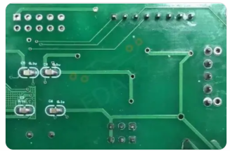
Analog signal wiring requirements
The main feature of the analog signal is poor anti-interference, and the protection of the analog signal is mainly considered when wiring.
The processing of analog signals is mainly reflected in the following points:
1. In order to increase its anti-interference ability, the wiring should be as short as possible.
2. Some analog signals can give up the impedance control requirement, and the wiring can be thickened appropriately.
3. Limit the wiring area, try to complete the wiring in the analog area, away from the digital signal.
High-speed PCB signal wiring requirements
1. Multilayer wiring
High-speed signal wiring circuits tend to have high integration and high wiring density. The use of multi-layer boards is not only necessary for wiring, but also an effective means to reduce interference. Reasonable selection of the number of layers can greatly reduce the size of the printed board, and can make full use of the intermediate layer to set up the shield, which can better realize the nearby grounding, can effectively reduce the parasitic inductance, can effectively shorten the signal transmission length, and can greatly reduce the signal Cross-interference and so on.
2. The less lead bends, the better

The less the lead bends between the pins of the high-speed circuit device, the better. The lead wire of high-speed signal wiring circuit wiring is best to adopt a full straight line, which needs to be turned. It can be turned by 45° broken line or circular arc. This requirement is only used to improve the fixing strength of the steel foil in low-frequency circuits, while in high-speed circuits, it can meet this requirement. One requirement can reduce the external emission and mutual coupling of high-speed signals, and reduce signal radiation and reflection.
3. The shorter the lead, the better
The shorter the lead between the pins of the high-speed signal wiring circuit device, the better. The longer the lead, the larger the distributed inductance and distributed capacitance, which will have a lot of influence on the passage of high-frequency signals of the system. At the same time, it will also change the characteristic impedance of the circuit, causing the system to reflect and oscillate.
4. The less alternating between lead layers, the better
The fewer lead layers alternate between pins of high-speed circuit devices, the better. The so-called "the less the inter-layer alternation of the leads, the better" means that the fewer vias used in the component connection process, the better. It is measured that one via can bring about 0.5pf of distributed capacitance, leading to a significant increase in the delay of the circuit, and reducing the number of vias can significantly increase the speed.
5. Pay attention to parallel cross interference
High-speed signal wiring should pay attention to the "cross-interference" introduced by the close parallel routing of signal lines. If parallel distribution cannot be avoided, a large area of "ground" can be arranged on the opposite side of the parallel signal lines to greatly reduce interference.
6. Avoid branches and stumps
High-speed signal wiring should try to avoid branching or forming tree stumps (Stub). Tree stumps have a great influence on impedance, which can cause signal reflection and overshoot, so we usually should avoid stumps and branches when designing. Using daisy chain wiring will reduce the impact on the signal.
How to wire PCB key signals
7. Try to go to the inner layer of the signal line
High-frequency signal lines on the surface are prone to generate large electromagnetic radiation, and are also susceptible to interference from external electromagnetic radiation or factors. Wire the high-frequency signal line between the power supply and the ground wire, and the radiation generated by the power supply and the bottom layer will be absorbed by electromagnetic waves.
Clock signal wiring requirements
In digital circuit design, a clock signal is a signal that oscillates between a high state and a low state, which determines the performance of the circuit. The clock circuit has an important position in the digital circuit, and at the same time is the main source of electromagnetic radiation. The clock processing method also needs special attention when PCB layout. The clock tree is clarified at the beginning, and the relationship between various clocks is clarified, so that it can be handled better when wiring. In addition, the clock signal is often a difficult point in EMC design, and special attention should be paid to items that require EMC test indicators.
In addition to the conventional impedance control and equal length requirements of the clock line, the following issues need to be paid attention to:
1. Try to choose the optimal wiring layer for the clock signal.
2. Try not to cross the division of the clock signal, let alone route it along the division area.
3. Pay attention to the distance between the clock signal and other signals, at least 3W.
4. For the design with EMC requirements, the inner layer wiring should be selected as far as possible when the line is longer.
5. Pay attention to the termination matching of the clock signal.
6. Do not use a daisy chain structure to transmit clock signals, but a star structure, that is, all clock loads are directly connected to the clock power driver.
7. All wires connected to the input/output terminals of the crystal oscillator should be as short as possible to reduce noise interference and the influence of distributed capacitance on the crystal oscillator.
8. The crystal capacitor ground wire should be connected to the device with the widest and shortest wire possible; the digital ground pin closest to the crystal oscillator should minimize vias.
9. In digital circuits, the usual clock signals are signals with fast edge changes and high external crosstalk. Therefore, in the design, the clock line should be surrounded by ground wires and ground wires should be used to reduce the distributed capacitance, thereby reducing crosstalk; for high-frequency signal clocks, try to use low-voltage clock signals and wrap the ground mode, and pay attention to the grounding. Hole integrity.
Differential signal wiring requirements
Differential signals, some of which are also called differential signals, use two exactly the same signals with opposite polarities to transmit one data, and the decision depends on the level difference of the two signals. In order to ensure that the two signals are exactly the same, they must be kept parallel when wiring, and the line width and line spacing remain unchanged.
How to route key signals in PCB design
On the circuit board, the differential traces must be two lines of equal length, equal width, close proximity, and on the same level.
1. Equal length: Equal length means that the length of the two lines should be as long as possible, in order to ensure that the two differential signals keep opposite polarities at all times. Reduce common mode components.
2. Equal width and equal distance: Equal width means that the trace width of two signals needs to be kept the same, and equal distance means that the distance between the two lines should be kept constant and parallel.
Reminder: Try to provide dedicated wiring layers for key signals such as clock signals, high-frequency signals, and sensitive signals, and ensure the smallest loop area. Use methods such as shielding and increasing the safety distance to ensure signal quality.