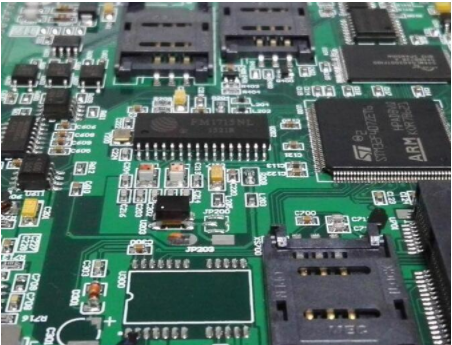
In the process of PCB circuit board production, soldering is an indispensable and important process. After the circuit board is soldered, it is sometimes found that there are white residues on the circuit board, which affects the aesthetics of the circuit board and may affect the performance of the circuit board. Therefore, it is necessary to understand the causes of these white residues and deal with them.
The reason and treatment method of white residue after PCB circuit board soldering:
1. The appearance of white residues is generally caused by improper use of flux. Rosin-based fluxes often cause white spots during cleaning. Sometimes this phenomenon will not occur when switching to other types of flux.
2. If there are residues on the circuit board during the production of the circuit board, white spots will occur after storage for a long time, and a strong solvent can be used to clean it.
3. Incorrect handling of circuit boards will also cause white spots. Often a certain batch of circuit boards will have problems, but others will not. For this phenomenon, use a strong solvent to clean it.
4. The flux was incompatible with oxidation maintenance. Just use another flux to improve the problem.
5. Because the solvent in the manufacturing process degrades the raw materials of the PCB board, there will also be white residues, so the shorter the storage time, the better. The solution in the nickel plating process often causes this problem, which requires special attention.
6. The flux has been used for a long time and aged, and exposed to the air to absorb water and form white spots. When using fresh flux, the solder stays for too long before cleaning.
If a white residue appears after the PCB board is soldered, it needs to be treated seriously, analyze the cause, and solve it in a targeted manner. Only in this way can the PCB circuit board have good performance and a clean appearance.
Summary of practical skills in high-frequency PCB design

The goal of PCB design is smaller, faster and lower cost. And because the interconnection point is the weakest link in the circuit chain, in the RF design, the electromagnetic properties at the interconnection point are the main problems faced by the engineering design. Each interconnection point must be investigated and the existing problems must be solved. The interconnection of the circuit board system includes three types of interconnection: the chip to the circuit board, the interconnection within the PCB board, and the signal input/output between the PCB and external devices. This article mainly introduces a summary of practical techniques for high-frequency PCB design with interconnections within the PCB board. I believe that understanding this article will bring convenience to future PCB design.
In the PCB design, the interconnection of the chip and the PCB is important for the design. However, the main problem of the interconnection between the chip and the PCB is that the interconnection density is too high, which will cause the basic structure of the PCB material to become a factor limiting the growth of the interconnection density. This article shares practical tips for high-frequency PCB design. As far as high-frequency applications are concerned, the techniques for high-frequency PCB design with interconnections within the PCB board are:
The corner of the transmission line should be 45° to reduce the return loss;
High-performance dielectric circuit boards whose dielectric constant values are strictly controlled according to the number of layers should be used. This method is conducive to effective simulation calculation of the electromagnetic field between the insulating material and the adjacent wiring.
The PCB design specifications related to high-precision etching must be specified. It is necessary to consider that the total error of the specified line width is +/-0.0007 inches, the undercut and cross-section of the wiring shape should be managed, and the plating conditions of the wiring side wall should be specified. The overall management of wiring (wire) geometry and coating surface is very important to solve the skin effect problem related to microwave frequency and realize these specifications.
The protruding pin leads have tap inductance and parasitic effects, so avoid using components with leads. In high frequency environments, it is best to use surface mount SMD components.
For PCB signal vias, avoid using the via processing (pth) process on the PCB sensitive board, because this process will cause lead inductance at the vias. For example, when a through hole on a 20-layer board is used to connect layers 1 to 3, there are 4 to 19 layers of lead inductance, and buried blind holes or back drills should be used.
To provide a rich ground plane. Use molded holes to connect these ground planes to prevent the 3D electromagnetic field from affecting the circuit board.
To choose electroless nickel plating or immersion gold plating process, do not use HASL method for electroplating. This kind of electroplated surface can provide better skin effect for high frequency current. In addition, this highly solderable coating requires fewer PCB leads, which helps reduce environmental pollution.
The solder mask prevents the flow of solder paste. However, due to the uncertainty of thickness and the unknown of dielectric constant performance, covering the entire board surface with solder mask material will cause changes in circuit performance in the PCB microstrip design. Generally, a solder dam (solderdam) is used as the solder mask.