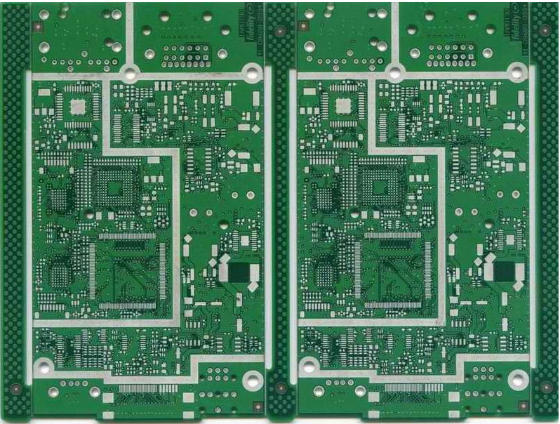
The ambient lighting source of the PCB lithography process is yellow light, rather than the red light of the general photography darkroom, so this process is often referred to as the "yellow light" process.
The yellow light process can be divided into PR coating, exposure, development and etching to obtain the required circuit pattern.
FPC yellow light process
Prevent foreign matter from remaining on the copper surface and cause poor PCB circuit.
Increasing the roughness of the copper surface is conducive to the combination of the copper surface and the photosensitive film.
Reaction mechanism:
Micro etching bath potion: AD485 (Na2S2O8 + stabilizer), H2SO4
Na2S2O8+Cu=Na2SO4+CuSO4
CuO+H2SO4=CuSO4+H20
Control concentration:
AD485: 50-80g/L Cu2+: 10g/L photosensitive film lamination
Paste a photosensitive film on the substrate to prepare for the formation of the circuit. Photosensitive film composition: photosensitive film process:
Hot pressing and rolling effect: The photosensitive film and the substrate are fully pressed by temperature and pressure, and the pressing temperature is 100-110°C. The pressure is 0.3Mp
The function of the vacuum chamber: to prevent the formation of foreign matter and bubbles in the photosensitive film. The vacuum degree is 95-105
High-precision exposure (exposure)

The UV light is irradiated on the photosensitive film that needs to form the circuit through the specified glass mask to cure it
Process flow:
illustrate
The exposed version of GLASS MASK is divided into a large board and a small board, and the corresponding exposure machines are also different.
By controlling the development time, the development can be achieved with a weak alkali developer
mechanism:
Dissolve the exposed part of the (positive) photoresist in the developer quickly, and slowly dissolve the unexposed part
Dissolution (negative photoresist is just the opposite, the exposed part slowly dissolves in the developer, and the unexposed part dissolves quickly). Commonly used developer sodium carbonate 6.5-7.0g/L
Etching
Dissolve copper with etching solution (ferric chloride, copper chloride, etc.)
Etching factor:
During the etching process, the etching solution not only produces an etching effect on the left and right directions but also downward, and side etching is inevitable. The ratio of the side etching width to the etching depth is called the etching factor. It is impossible to completely eliminate side erosion in the industry at present, and we can only minimize it. Usually by changing the pressure, speed, temperature and other parameters to change the amount of side erosion.
Tailun FPC protective film introduction
High temperature bearing film:
Applied to Panel To Panel process, PCB single-sided board is pasted with dry film on the copper surface, and at the same time a carrier film is pasted on the PI surface
Repost film:
Small piece of auxiliary materials for reposting is mainly for small-area auxiliary materials, including cover film, reinforcement, shielding film or other pressure-sensitive auxiliary materials for reposting. Effectively improve processing efficiency and product yield.
Die-cut load-bearing film:
Before punching the shape of the FPC, it is first attached to the PET film coated with weak adhesion, and then the half-cut shape processing (embedded punching) is performed with a knife die, and it is left to the user intact, and the user can put the FPC Take it down and assemble it, you can also assemble it first, and then take it off from the PET film after the assembly is complete.
Shipment protective film:
The surface protection material with the function of preventing FPC from being damaged, using PET with a certain stiffness as the base material, meeting different viscosity requirements, product series surface protection material. Separate the PCB double-layer packaging film, fix the sticky side on the table, arrange the products neatly on the sticky PET double-layer packaging film, stick the release film after it is fully glued, and flatten it by hand. After wrapping a stack, place FR2 partitions on the upper and lower layers to fix it. Pack it in a big plastic bag, seal it with a sealer, paste qualified labels, and pack it into the warehouse.