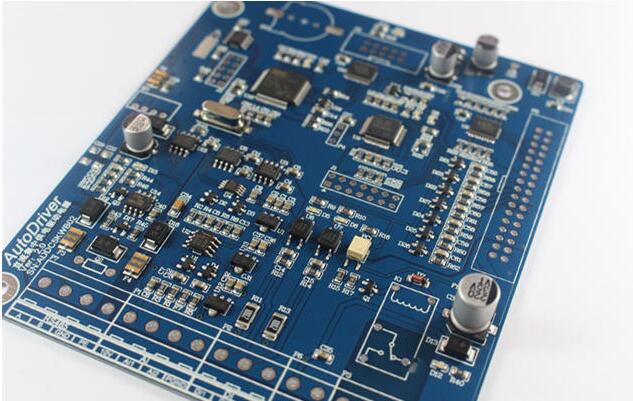
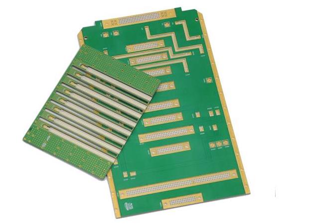
Process requirements for PCBA mounting components:
(1) The type, model, nominal value and polarity of each assembly tag component must conform to the requirements of the product assembly drawing and schedule.
(2) The mounted components must be intact.
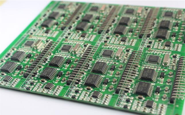
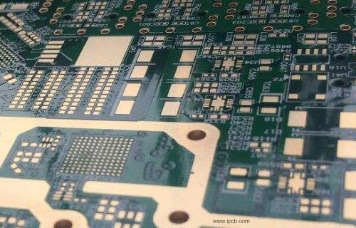
(3) The solder ends or pins of the mounted components should invade the solder paste with a thickness of not less than 1/2. For general components, the amount of solder paste extrusion (length) should be less than 0.2mm. For narrow-pitch components The amount of solder paste squeezed out of the film (the length should be less than 0.1m).
(4) The ends or pins of the PCB components are aligned and centered with the land pattern. Because the PCB circuit board has a self-positioning effect during flow soldering, there will be a certain deviation in the placement position of the components, and the allowable deviation range is required. as follows:
Rectangular components: Under the condition that the PCB board pad is designed correctly, the width of the component's width direction solder end width is more than 3/4 on the pad. After the component's solder end overlaps the pad in the length direction of the component, the pad extends The output part should be greater than 1/3 of the height of the solder tip: when there is a rotation deviation, more than 3/4 of the width of the component solder tip must be on the pad.

When mounting, pay special attention to the component solder tip must be in contact with the solder paste.
Small outline transistor (SOT): Allow x, Y, T (rotation angle) deviation, but the pins must all be on the PCB pad.
Small outline integrated circuit (SOTC): allow x, Y, T (rotation angle) to have mounting deviation, but must ensure that 3/4 of the component pin width is on the PCB circuit board pad.
Quad flat package components and ultra-small package devices (QFP): It is necessary to ensure that the 34 of the pin width is on the PCB circuit board pad, allowing small mounting deviations for X, Y, and T.
The components are correct
It is required that the type, model, nominal value and polarity of each assembly tag component must meet the requirements of the product assembly drawing and schedule, and the wrong position must not be pasted.
Accurate location
(1) The ends or pins of the components and the land pattern should be aligned and centered as much as possible, and the components should be soldered to contact the solder paste.
(2) The placement of components must meet the process requirements.
The self-positioning effect of the Chip components at the two ends is relatively large. During placement, the component width of 12~3/4 or more is overlapped on the PCB circuit board pad, and the two ends in the length direction only need to be overlapped to the corresponding PCB. On the circuit board pad and contact the solder paste pattern, it can self-position during flow soldering, but if one of the ends is not connected to the PCB circuit board pad or does not touch the solder paste pattern, it will be generated during reflow soldering The condition of the displacement or suspension bridge.
For SOP, SOJ, OFP, PLCC and other devices, the self-positioning effect is relatively small, and the placement offset cannot be corrected by reflow soldering; if the placement position exceeds the allowable deviation range, the smt technical operator must manually correct it afterwards. Enter the reflow soldering furnace for welding. Otherwise, it must be repaired after reflow soldering, which will cause the PCB manufacturer's extreme waste of man-hours and materials, and even affect the reliability of product quality. If the mounting position is found to exceed the allowable range during PCB processing and production, the mounting coordinates should be corrected in time.
Manual placement or manual timing requires the placement of accurate placement, pin and pad aligned, centered, be sure to pay attention if placement is not correct, drag on the solder paste to align, one side of the solder paste pattern adhesion, causing bridging.
The pressure (patch height) is appropriate, and the patch pressure (Z-axis height) is appropriate.
The placement pressure is too small, the solder ends or pins of the components are on the surface of the solder paste, the solder paste cannot stick to the components, and the position shifts intentionally during transfer and reflow. In addition, because the Z axis is too high, the components are placed Throwing it from a high place will cause the placement of the patch to shift.
Excessive patch pressure and excessive solder paste extrusion will easily cause solder paste adhesion and bridging during reflow soldering. At the same time, the patch position will shift due to sliding, and components will be damaged in severe cases.