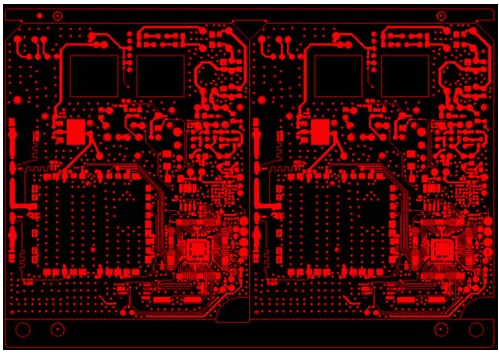
Now it is a sign: the PCB processing quality of punching, cutting, and drilling is inconsistent, the coating adhesion is poor, or the coating is uneven in the metallized hole.
Inspection method: Inspect the incoming materials, test various key mechanical PCB processing operations, and conduct routine analysis after the incoming materials are passed through the hole metallization process.
possible reason:
1. Material curing, resin content, or plasticizer changes will affect the quality of drilling, punching and shearing of the material.
2. Poor drilling, punching or shearing technology makes the production quality poor or inconsistent.
3. The preheating cycle time before punching or drilling is too long, which sometimes affects the PCB processing of the laminate.
4. The aging of materials, mainly phenolic materials, sometimes causes the plasticizer in the material to run away, making the material more brittle than usual.
Solution:

1. Contact the laminate manufacturer to establish a test that mimics the processing performance requirements of key mechanical PCBs. The production mold should not be used for the test, otherwise the wear and change of the production mold will affect the test results. In any problem of mechanical PCB processing performance changes, only when the problem occurs at the same time as the material batch number change, can the quality of the laminate be suspected.
2. Refer to the manufacturing recommendations for various types of laminates. Contact the laminate manufacturer to find out the specific drilling speed, feed, bit and punch temperature for each grade of laminate. Remember: every manufacturer uses a different mixture of resins and substrates, and their recommendations will vary.
3. Carefully preheat the laminate, be sure to find any overheated areas, such as those under a heating lamp. When heating materials, the first-in first-out principle should be observed.
4. Inspect with the laminate manufacturer to obtain the aging characteristics data of the material. Turnover inventory, so that inventory is usually newly produced plates. Be sure to find out possible overheating in warehouse storage.
Four. Warpage and distortion problems
It is now a sign: no matter before, after or during PCB processing, the substrate is warped or distorted. The tilt of the hole after soldering is also a sign of warpage and distortion of the substrate.
Inspection method: use float welding test, it is possible to carry out incoming material inspection. The 45-degree tilted soldering test is particularly effective.
possible reason:
1. At the time of receipt or after sawing and cutting, the material is warped or twisted, which is usually caused by improper lamination, improper cutting or unbalanced laminate structure.
2. Warpage can also be caused by improper storage of materials, especially paper-based laminates. When they are placed upright, they will be bowed or deformed.
3. Warpage is caused by unequal copper wall and iron wall foils, such as 1 ounce on one side and 2 ounces on the other side: the electroplating layer is not equal, or the special printed board design causes copper stress or thermal stress.
4 Improper fixture or fixation during soldering, and heavy components during soldering operations can also cause warpage.
5. In the process of PCB processing or soldering process, the hole displacement or tilt on the material is caused by improper curing of the laminate or the stress of the substrate glass cloth structure.
Solution:
1. Straighten the material or release the stress in the oven, and perform the cutting operation according to the inclination angle and the heating temperature of the board recommended by the laminate manufacturer. Contact the laminate manufacturer to ensure that substrates with uneven structures are not used.
2. Store the material flat in the loading cardboard box or lay the material diagonally flat on the shelf. Generally, the material should be placed at an angle of 60 degrees or less with the ground.
3. Contact the laminate manufacturer to avoid unequal copper foils on both sides. Analyze plating and stress, or local stress caused by heavy components or large copper foil area. Redesign the printed board to balance the components and copper area. Sometimes most of the wires on one side of the printed board and the wires on the other side are laid vertically, so that the thermal expansion of the two sides is not equal and cause distortion. As long as possible, this kind of wiring should be avoided.
4. In the soldering operation, printed boards, especially paper-based printed boards, must be clamped with clamps. In some cases, heavy components must be balanced with special fixtures or fixtures.
5. Contact the laminate manufacturer and use any recommended post-curing measures. In some cases, PCB laminate manufacturers will recommend another laminate for more stringent or special applications.