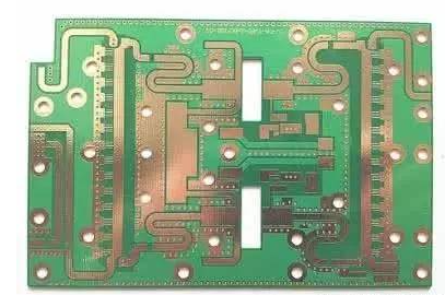
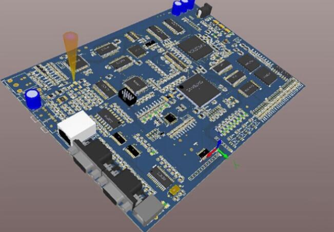
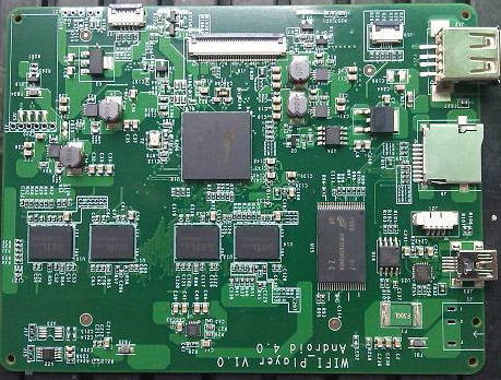
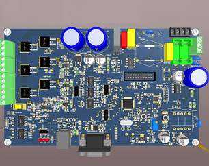
Introduce the PCBA process of different types of PCB boards
1. Single-sided SMT mounting
The solder paste is added to the component pad, after the solder paste printing of the bare PCB is completed, the relevant electronic components are mounted through reflow soldering, and then reflow soldering is performed.
2. Single-sided DIP cartridge
The PCB board that needs to be plug-in is wave soldered by the production line workers after inserting the electronic components. After the soldering is fixed, the feet can be cut to wash the board, but the wave soldering production efficiency is low.
3. Single-sided mixed
The PCB board is printed with solder paste, and the electronic components are mounted and fixed by reflow soldering. After the quality inspection is completed, DIP insertion is performed, and then wave soldering or manual soldering. If there are few through-hole components, manual soldering is recommended .

4. Single-sided mounting and plug-in mixing
Some PCB boards are double-sided, one side is mounted and the other side is inserted. The process flow of mounting and inserting is the same as single-sided processing, but the PCB board requires the use of fixtures for reflow soldering and wave soldering.
5. Double-sided SMT mounting
In order to ensure the aesthetics and functionality of the PCB board, some PCB board design engineers will adopt a double-sided mounting method. IC components are arranged on side A and chip components are mounted on side B. Make full use of the PCB board space and realize the miniaturization of the PCB board area.
6. Double-sided mixed
The following two methods are mixed on both sides:
The first method PCBA assembly is heated three times, the efficiency is low, and the pass rate of wave soldering using the red glue process is low, and it is not recommended.
The second method is suitable for cases where there are many double-sided SMD components and few THT components. Manual welding is recommended. If there are many THT components, wave soldering is recommended.
What issues should be considered in the assembly of PCBA
The solder paste printing process mainly solves the problem of the consistency of the solder paste printing volume (filling and transfer), rather than the demand for the volume of solder paste for each solder joint. In other words, the solder paste printing process solves the problem of fluctuations in soldering through rate, not the problem of high and low through rate. To solve the problem of pass-through rate, the key lies in the distribution of solder paste. Through the optimization and matching design of pads, solder mask and stencil opening, the amount of solder paste is allocated to each solder joint as needed. Of course, the consistency of the amount of solder paste is also related to the design, and different designs of PCB solder mask provide different process capability indexes.
1. Area ratio
The area ratio refers to the ratio of the area of the steel mesh window to the area of the window hole wall
2. Transfer rate
The transfer rate refers to the ratio of the solder paste deposited on the pads in the stencil window during printing, expressed by the ratio of the amount of solder paste actually transferred to the volume of the stencil window.
3. The effect of area ratio on transfer rate
The area ratio is an important factor that affects the transfer of solder paste. Generally, the area ratio is required to be greater than 0.66 in engineering. Under this condition, a transfer rate of more than 70% can be obtained.
4. Design requirements for area comparison
The area ratio has requirements for the design of the steel mesh, which mainly affects the fine-pitch components. In order to ensure the area ratio of the micro-pad stencil window, the thickness of the stencil must meet the area ratio requirement. In this way, for components that require a large amount of solder paste, it is necessary to increase the amount of solder paste by increasing the stencil window area-this requires space for deformation around the PCB pad, which is a major consideration in the design of component spacing.