To make a PCB board is to turn the designed schematic diagram into a real PCB circuit board. Please don't underestimate this process. There are many things that work in principle but are difficult to achieve in engineering, or others can achieve. Some people can't realize it, so it is not difficult to make a PCB board, but it is not easy to make a PCB board well.
The two major difficulties in the field of microelectronics are the processing of high-frequency signals and weak signals. In this regard, the level of PCB production is particularly important. The same principle design, the same components, and PCBs produced by different people have different results., Then how can we make a good PCB board? Based on our past experience, I would like to talk about my views on the following aspects:
1. Make clear design goals

Receiving a design task, we must first clarify its design goals, whether it is an ordinary PCB board, a high-frequency PCB board, a small signal processing PCB board, or a PCB board with both high frequency and small signal processing. If it is an ordinary PCB board, As long as the layout and wiring are reasonable and tidy, and the mechanical dimensions are accurate, if there are medium load lines and long lines, certain measures must be used to reduce the load, and the long line must be strengthened to drive, and the focus is to prevent long line reflections. When there are more than 40MHz signal lines on the board, special consideration should be given to these signal lines, such as crosstalk between lines. If the frequency is higher, there is a stricter limit on the length of the wiring. According to the network theory of distributed parameters, the interaction between the high-speed circuit and its wiring is a decisive factor and cannot be ignored in system design. As the transmission speed of the gate increases, the opposition on the signal lines will increase accordingly, and the crosstalk between adjacent signal lines will increase proportionally. Generally, the power consumption and heat dissipation of high-speed circuits are also very large, so we are doing high-speed PCB s. Enough attention should be paid.
When there are millivolt or even microvolt-level weak signals on the board, these signal lines need special attention. Small signals are too weak and are very susceptible to interference from other strong signals. Shielding measures are often necessary, otherwise they will Greatly reduce the signal-to-noise ratio. As a result, the useful signal is submerged by noise and cannot be extracted effectively.
The commissioning of the board should also be considered in the design stage. The physical location of the test point, the isolation of the test point and other factors cannot be ignored, because some small signals and high-frequency signals cannot be directly added to the probe for measurement.
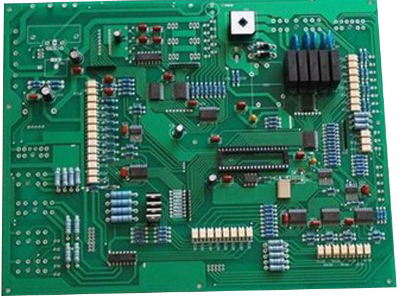
In addition, other relevant factors should be considered, such as the number of layers of the board, the package shape of the components used, and the mechanical strength of the board. Before making a PCB board, it is necessary to have a good idea of the design goals of the design.
Second, understand the requirements of the layout and routing of the functions of the components used
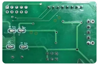
Some special components have special requirements in the layout and wiring, such as the analog signal amplifiers used in LOTI and APH. The analog signal amplifiers require stable power and small ripple. Keep the analog small signal part as far away from the power device as possible. On the OTI board, the small signal amplifying part is also specially equipped with a shielding cover to shield the stray electromagnetic interference. The GLINK chip used on the NTOI board uses the ECL process, which consumes a lot of power and generates heat. Special consideration must be given to the heat dissipation problem in the layout. If natural heat dissipation is used, the GLINK chip should be placed in a place with relatively smooth air circulation., And the heat radiated can not have a big impact on other chips. If the board is equipped with speakers or other high-power devices, it may cause serious pollution to the power supply. This point should also be paid enough attention.
three. Component layout considerations
The first factor that must be considered in the layout of components is electrical performance. Put closely connected components together as much as possible. Especially for some high-speed lines, make it as short as possible during layout, power signal and small signal components. To be separated. On the premise of meeting the performance of the PCB circuit board, the components must be placed neatly, beautifully, and easy to test. The mechanical size of the board and the location of the socket must also be carefully considered.