Nowadays, the development of electronic technology is very rapid. People cannot live without electronic products. Almost all electronic products need the support of PCB. Printed circuit board, or PCB, is an important electronic component, a support for electronic components, and a provider of circuit connections for electronic components. It is a product with a very high market share in the global electronic component products. The PCBA processing means that the empty PCB board goes through the SMT loading, and then goes through the entire manufacturing process of the DIP plug-in. Many people do not understand the materialization and development of PCBA processing.
PCBA processing

PCBA is the abbreviation of Printed Circuit Board Assembly in English, referred to as PCBA. This is a common way of writing in China, while the standard way of writing in Europe and America is PCB'A, with "'" added, which is called the official idiom.
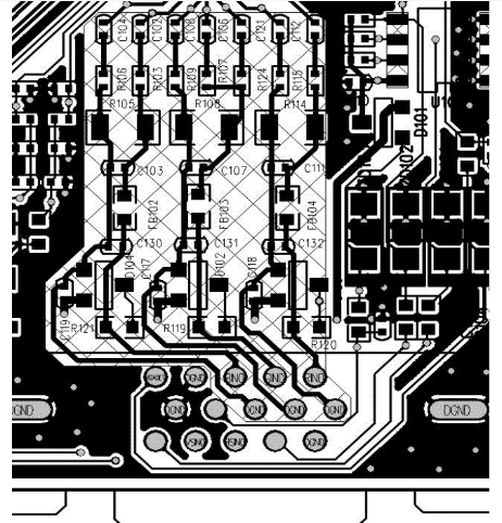
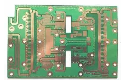
At the end of the 1990s when numerous build-up printed circuit board solutions were proposed, build-up printed circuit boards have also been put into practical use in large numbers until now. It is important to develop a robust test strategy for large, high-density printed circuit board assemblies (pcba, printed circuit board assembly) to ensure compliance and functionality with the design. In addition to the establishment and testing of these complex assemblies, the price of a single investment in electronic components may be very high, and may reach US$25,000 when a unit is tested later. Due to such high costs, finding and repairing assembly problems is now an even more important step than in the past. Today's more complex assembly is about 18 square inches, 18 layers; there are more than 2,900 components on the top and bottom sides; it contains 6,000 circuit nodes; there are no less than 20,000 solder joints to be tested.
New development projects require more complex,larger PCBs and tighter packaging. These requirements challenge the ability to build and test these units. Furthermore, larger circuit boards with smaller components and higher node counts may continue. For example, a design that is currently drawing a circuit board diagram has about 116,000 nodes, more than 5,100 components, and more than 37,800 solder joints that require testing or verification. This unit also has BGA on the top and bottom surfaces, and the BGA is next to each other. Using a traditional needle bed to test a board of this size and complexity, a method of ICT is impossible.
In the manufacturing process, especially in testing, the ever-increasing complexity and density of PCBs are not a new issue. Realizing that increasing the number of test pins in the ICT test fixture is not the direction to go, I started to observe alternative circuit verification methods. Looking at the number of non-contact probes per million, it is found that at 5000 nodes, many of the errors found (less than 31) may be due to probe contact problems rather than actual manufacturing defects (Table 1). Therefore, set out to reduce the number of test pins, rather than increase them. Nevertheless, the quality of the manufacturing process is evaluated to the entire PCBA. Decided to use a combination of traditional ICT and X-ray layering is a feasible solution.