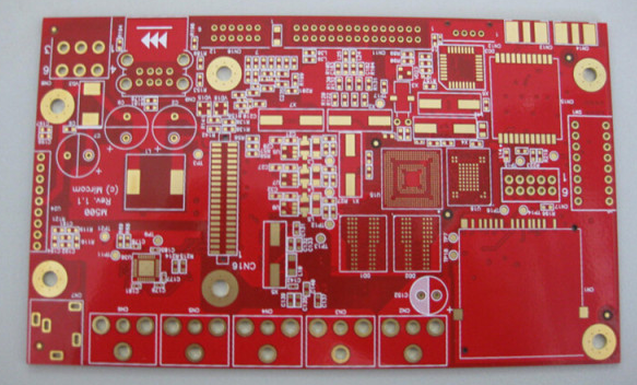
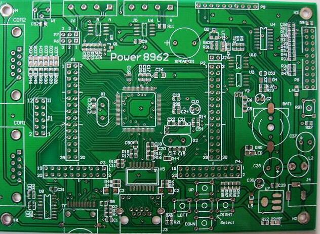
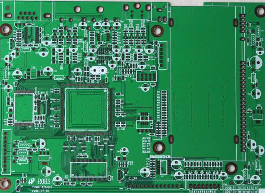
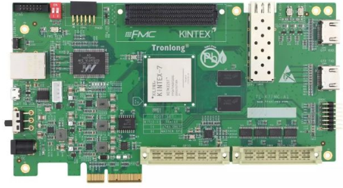
When PCBA is processed, a pre-production meeting must be held first, and the electronic components provided by PCBA must be purchased and inspected. A special PCBA incoming inspection station must be set up to strictly check the following items to ensure that the components are fault-free. Only in this way can the quality be guaranteed, without a lot of rework and repair work, then I will introduce the relevant content in detail.
1. How to control the quality of PCBA processing
1. It is particularly important to hold a pre-production meeting after receiving an order for processing PCBA. It is mainly the process of analyzing PCBGerber files and submitting manufacturability reports (DFM) according to different customer needs. Many small manufacturers do not pay much attention to this. But this is often the case. It is not only easy to cause quality problems due to poor PCB design, but also a lot of rework and repair work.

2. Purchase and inspection of electronic components provided by PCBA
The procurement channels of electronic components must be strictly controlled, and goods must be obtained from large traders and original manufacturers to avoid the use of second-hand materials and counterfeit materials. In addition, it is necessary to set up a special PCBA incoming inspection station to strictly check the following items to ensure that the components are fault-free.
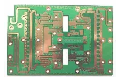
PCB: Check the temperature test of the reflow oven, whether the through holes without flying leads are blocked or leaking, whether the surface of the board is bent, etc.
IC: Check whether the screen printing is exactly the same as the screen printing. BOM and store it under constant temperature and humidity.
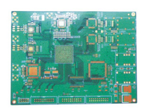
3. SMT assembly
Solder paste printing and reflow oven temperature control systems are key points in assembly, and laser templates with higher quality requirements and higher processing requirements are required. According to the needs of PCB, some need to increase or reduce the steel mesh or U-shaped holes, only need to make the steel mesh according to the process requirements. Among them, the temperature control of the reflow oven is very important for the wetting of the solder paste and the firmness of the steel mesh, and can be adjusted according to the normal SOP operation guide. In addition, strict implementation of AOI testing can greatly reduce defects caused by human factors.
4. Plug-in processing
In the plug-in process, the mold design of wave soldering is the key. PE engineers must continue to practice and summarize how to use molds to maximize productivity.
5. PCBA processing board test
For orders with PCBA test requirements, the main test content includes ICT (circuit test), FCT (functional test), combustion test (aging test), temperature and humidity test, drop test, etc.
2. Matters needing attention in PCBA processing
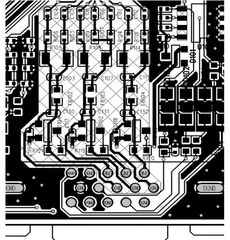
1. The minimum distance between the copper foil and the board edge is 0.5mm, the minimum distance between the component and the board edge is 5.0mm, and the minimum distance between the pad and the board edge is 4.0mm.
2. The minimum gap between copper foils is 0.3mm for single-sided boards and 0.2mm for double-sided boards. (Pay attention to the components of the metal shell when designing the double panel. The shell needs to be in contact with the PCB board when plugging in. The top pad cannot be opened, and it must be sealed with silk screen oil or solder mask.)
3. Jumpers are not allowed to be placed under the IC or under the components of potentiometers, motors and other large-volume metal casings.
4. The electrolytic capacitors are not allowed to touch the heating components. Such as transformers, thermistors, high-power resistors, radiators. The minimum distance between the radiator and the electrolytic capacitor is 10mm, and the distance between the remaining components and the radiator is 2.0mm.
5. Large components (such as transformers, electrolytic capacitors with a diameter of 15mm or more, and high-current sockets.) need to increase the pad.
6. Minimum line width: 0.3mm for single-sided board and 0.2mm for double-sided board (the minimum copper foil on the side is also 1.0mm).
7. There should be no copper foil (except for grounding) and components (or as required by the structure drawing) within 5mm of the screw hole radius.
8. The pad size (diameter) of the general through-hole mounting component is twice the aperture. The minimum size of the double-sided board is 1.5mm, and the minimum of the single-sided board is 2.0mm. (If round pads cannot be used, round pads can be used.