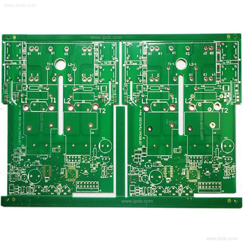
After PCB factories began to require the company’s products to use [Strain gage] to measure the bending effects of stress on PCBA many years ago, now [Strain gauge] measurement has become one of the PCB company’s product process inspection standards, even RD Most of them have accepted [Strain gage] as one of the design reference indicators, but most of them are still limited to the verification of process stress. The next step I want to promote is to implement [Strain gauge] to DQ tumble test and drop During the drop test.
The purpose is to verify how severe the bending strain of the internal circuit board is caused by the impact of the product during the rolling and drop test. This is the RD that should verify the design parameters. Otherwise, even if the PCB manufacturing factory tries hard to make the circuit The strain on the board during the assembly process is minimized, but the PCB products are hung up as soon as they land on the customer's hands. Such products should be miserable when they are sold on the market!
I want to push the [Strain gage] measurement to the direction of research and development. In fact, it has the selfishness of Shenzhen Grand Power, because every time RD encounters the problem of BGA solder ball cracking, the first reaction is to look back. The department requested to see whether the solder strength can be strengthened to resist solder cracking.

No matter how painful the explanation is, no matter how hard the solder strength is, it cannot be strengthened to fully resist the stress caused by the bending of the board when the product falls. Means to solve the problem of plate bending caused by impact stress, so the previous series of "electronic parts falling or tin cracking must be a myth in the SMT process?" 】The article appears.
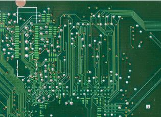
What I finally got in exchange was the development and design of a shielding-can that was integrally formed and directly welded to the circuit board. The purpose was to strengthen the board's rigidity to resist the bending problem caused by impact stress, but it was also required. The welding of the shielding cover cannot be offset to the edge of the soldering pad, otherwise an effective solder arc (fillet) cannot be formed on the edge of the shielding frame, and the shielding cover is not allowed to be used as a positioning pin. It is not easy to produce and maintain the shielding cover directly on the circuit board without mentioning it. "The shielding cover is not allowed to shift to the edge of the soldering pad." The SMT factory has strongly rebounded because the current equipment in the factory cannot effectively check the shielding 100%. The offset of the box.
The PCB engineer was required to personally measure the offset of a certain number of shielding cases under an optical microscope, and also to make slices to see that the fillet shape appeared on the inside and outside of the shielding case.
The engineer was required to personally measure the offset of a certain number of shielding covers under an optical microscope, and also to make slices to check the fillet shape of the inside and outside of the shielding cover.
For this reason, we also specifically asked the PCB engineer to personally measure the offset of a certain number of shielding cases under an optical microscope, and also to make slices to see the fillet shape on the inside and outside of the shielding case.