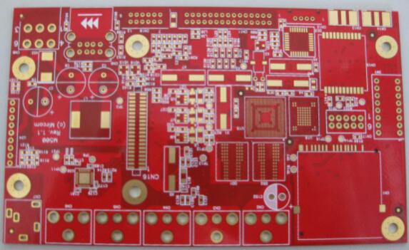
There is a common saying that "details determine success or failure". The distance between a PCB engineer novice and a veteran is often reflected in some details.
1. Pay attention to the placement direction and distance of the components on the edge of the PCB board
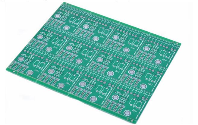
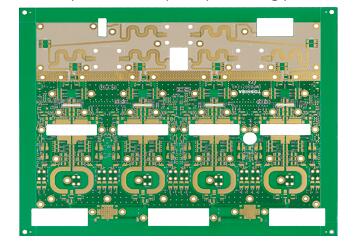
Since the PCB is generally made of jigsaw, the devices near the edge need to meet two conditions.
The first is to be parallel to the cutting direction (to make the mechanical stress of the device uniform. For example, if the device is placed in the way on the left side of the figure above, the different force directions of the two pads of the patch may cause the component and the welding to be split. Disk falls off)
The second is that components cannot be arranged within a certain distance (to prevent damage to components when the board is cut)
2. Pay attention to the spacing between patches

The spacing between SMD components is a problem that engineers must pay attention to during layout. If the spacing is too small, it is very difficult to print solder paste and avoid soldering and tinning.
The distance recommendations are as follows
Device distance requirements between patches:
Same kind of devices: ≥0.3mm
Dissimilar devices: ≥0.13*h+0.3mm (h is the maximum height difference of neighboring components)
The distance between components that can only be manually patched: ≥1.5mm.
The above suggestions are for reference only, and can be in accordance with the PCB process design specifications of the respective companies
3. Pay attention to the distance between wires or components and the edge of the board
Note that the leads or components should not be too close to the edge of the board, especially single-sided boards. Generally, single-sided boards are mostly paper boards, which are easy to break after being stressed. If you connect or place components on the edge, it will be affected.
4. The placement of decoupling capacitors for IC
A decoupling capacitor must be placed near the power port of each IC, and the location should be as close as possible to the power port of the IC. When a chip has multiple power ports, a decoupling capacitor must be placed on each port.
5. Treatment of line corners
Usually the thickness of the wire will change at the corners, but when the wire diameter changes, some reflections will occur. The corner method is the worst for the thickness change of the line, the 45-degree angle is better, and the rounded corner is the best. However, rounded corners are more troublesome for PCB design, so it is generally determined by the sensitivity of the signal. For general signals, a 45-degree angle is sufficient. Only those very sensitive lines need rounded corners.
6. It is best not to punch the via hole on the pad
Note that the through holes are best not to be punched on the pads, which can easily cause solder leakage.
7. The lead width on both sides of the component pad should be the same
The lead width on both sides of the component pad should be the same
8. Teardrops need to be added if the lead is smaller than the plug-in pad
If the wire is smaller than the pad of the in-line device, teardrops are needed.
Adding teardrops has the following benefits:
1. Avoid the sudden decrease of the signal line width and cause reflection, which can make the connection between the trace and the component pad tend to be smooth and transitional.
2. The problem that the connection between the pad and the trace is easily broken by impact is solved.
3. The setting of teardrops can also make the PCB circuit board look more beautiful.