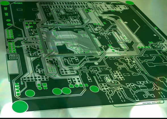
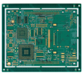
When a PCB board has completed the layout and routing PCB design, and checked the connectivity and spacing without errors, is a PCB board completed? The answer is of course no. Many beginners also include some experienced engineers. Due to time constraints or impatient or overconfidence, they often rashly and neglect the later inspections. As a result, some very basic bugs appeared, such as insufficient line width, component label silk screen pressed on vias, sockets too close, signal loops, and so on. As a result, electrical problems or process problems are caused, and the board must be re-printed in serious cases, resulting in waste. Therefore, after the layout and routing of a PCB board is completed, a very important step is post-inspection.
There are many detailed elements in the inspection of PCB boards. I have listed some of the elements that I think are the most basic and the most error-prone, as a later inspection.
1. Component packaging
(1) Pad pitch. If it is a new device, draw the component package yourself to ensure that the spacing is appropriate. The pad spacing directly affects the soldering of the components.

(2) Via size (if any). For plug-in devices, the size of the vias should be left with sufficient margin, generally not less than 0.2mm is more appropriate.
(3) Contour silk screen. The outline silk screen of the device should be larger than the actual size to ensure that the device can be installed smoothly.
2. Layout
(1) IC should not be near the edge of the board.
(2) The components of the same module circuit should be placed close to each other. For example, the decoupling capacitor should be close to the power supply pin of the IC, and the components that make up the same functional circuit should be placed in one area with a clear hierarchy to ensure the realization of the function.
(3) Arrange the position of the socket according to the actual installation. Sockets are all lead to other modules. According to the actual structure, in order to facilitate installation, the principle of proximity is generally adopted to arrange the position of the socket, and it is generally close to the edge of the board.
(4) Pay attention to the direction of the socket. The sockets are oriented, and if the direction is reversed, the wire must be re-customized. For flat sockets, the direction of the socket should be toward the outside of the board.
(5) There can be no devices in the Keep Out area.
(6) The source of interference should be far away from sensitive circuits. High-speed signals, high-speed clocks, or high-current switching signals are all interference sources and should be kept away from sensitive circuits, such as reset circuits and analog circuits. They can be separated by paving.
3. Wiring
(1) The size of the line width. The line width should be selected in combination with the process and the current carrying capacity, and the minimum line width cannot be less than the minimum line width of the PCB manufacturer. At the same time, to ensure the current carrying capacity, the appropriate line width is generally selected at 1mm/A.
(2) Differential signal line. For differential cables such as USB and Ethernet, please note that the cables should be of equal length, parallel, and in the same plane, and the spacing is determined by the impedance.
(3) Pay attention to the return path of the high-speed line. High-speed lines are prone to electromagnetic radiation. If the area formed by the routing path and the return path is too large, a single-turn coil will radiate electromagnetic interference outward. Therefore, when wiring, pay attention to the return path next to it. The multi-layer board is provided with a power layer and a ground plane to effectively solve this problem.
(4) Pay attention to the analog signal line. The analog signal line should be separated from the digital signal, and the wiring should try to avoid passing by interference sources (such as clocks, DC-DC power supply), and the wiring should be as short as possible.