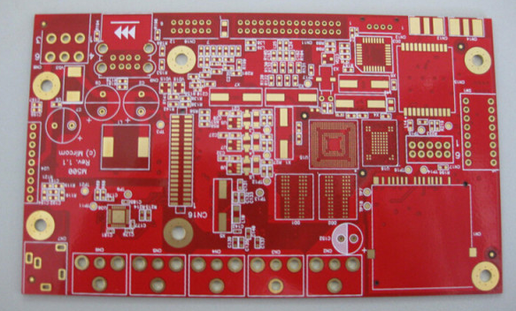
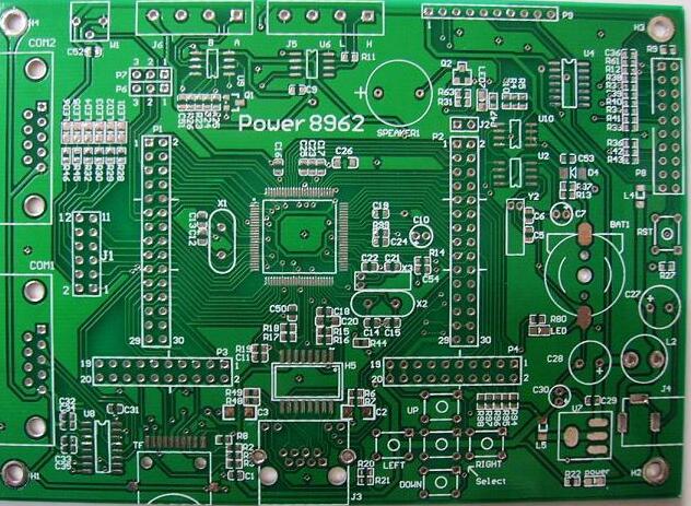
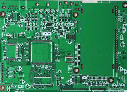
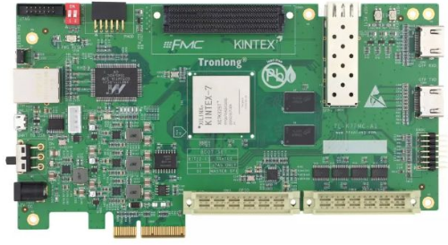
Lead-free PCBA processing refers to PCBA that does not use lead at any stage of manufacturing. Traditionally, lead is used in the PCB soldering process. However, lead is toxic and therefore harmful to humans. Considering its consequences, the EU Restriction of Hazardous Substances Directive (RoHS) prohibits the use of lead in PCBA processing. Substituting less toxic substances for lead has almost no difference in PCBA processing. This article introduces the lead-free PCBA process step by step in detail.
Lead-free PCBA guide
The lead-free PCBA processing process is divided into two basic parts, namely the pre-assembly process and the active assembly process. The steps involved in the lead-free PCBA process are as follows.
Pre-assembly steps
Lead-free PCB manufacturing involves three basic pre-assembly steps. These steps lay the foundation for error-free and accurate PCB assembly. The pre-assembly steps for lead-free PCB assembly are as follows.

analyze:
Analysis is a process similar to prototypes. The manufacturer uses the finished lead-free PCB as the prototype. This can be a normal operating PCB, an invalid PCB or a dummy component. The template used for assembly is traced by contour. Compare the lead-free component design with the prototype to ensure its compatibility with the component.
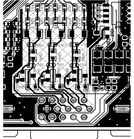
Solder paste inspection:
Since lead-free solder joints have a metallic appearance, which is very different from lead-based solders, careful inspection is very important. Check the PCB shape and solder paste in accordance with the IPC-610D standard to ensure that the lead-free solder joints are firm and firm. The moisture content was also tested in this step, because the circuit board is exposed to high moisture content in lead-free soldering compared to traditional soldering.
Bill of Materials (BOM) and component analysis:
During this process, the customer must verify the bill of materials (BOM) to ensure that the components are made of lead-free materials. Lead-free components are susceptible to moisture, so manufacturers should bake them in an oven. Once the necessary steps are performed, the actual lead-free assembly begins.
Active assembly steps
In the active assembly process, PCB assembly is actually carried out. The steps involved in active lead-free assembly are as follows.
Template placement and solder paste application:
In this step, the lead-free template of the forming stage is placed on the board. Then apply lead-free solder paste. Generally, the lead-free solder paste material is SAC305.
Component installation:
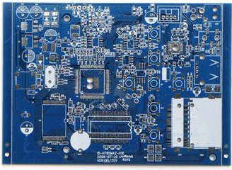
After applying solder paste, install the components on the board. Component placement can be done manually or using automatic machinery. This is a pick and place operation, but the components used need to be confirmed and marked during the BOM verification stage. The machine or operator selects the labeled components and places them in the designated locations.
Welding:
Perform lead-free through-hole or manual soldering at this stage. No matter which process is used, THT or SMT, soldering must be lead-free.
The circuit board placement in the reflow oven:
RoHS-compliant PCBs require high-temperature heating to evenly melt the solder paste. Therefore, the PCBs are placed in a reflow oven, where the solder paste is melted. In addition, the board is cooled at room temperature to solidify the molten solder paste. This helps to hold the component in its place.
Test and packaging:
PCB has been tested in accordance with the IPC-600D standard. In this step, the solder joints are tested. The visual inspection is followed by AOI and X-ray inspection. Perform physical and functional tests before packaging.
For the packaging of lead-free PCBs, it is very important to use anti-static discharge bags. This is very important to ensure that the final product is not subject to static charges during transportation.
However, despite having a thorough understanding of lead-free PCBA processing, it should still be improved by experts.