As a PCB engineer, you must master how to quickly design a successful PCB circuit board. This means that you are taking a fast and reliable professional quality PCB path.
This article will explore some of the simplicity applicable to printed circuit board (PCB) design novices and veterans, as long as they pay more attention to these skills in the design process. You can reduce the number of redesigns, shorten the design time, and reduce the diagnosis of the overall design results; the following are the issues we understand one by one.
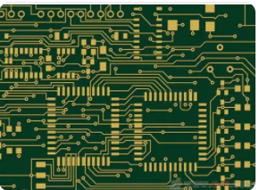
1. Familiar with the production process of the factory.
In this era of non-chip factory ICs, it is not surprising that many engineers do not know that PCB production steps and chemical treatment processes are produced according to their design documents. However, the lack of such real-world knowledge often leads novice engineers to make more complex design decisions.
Does the design really need to be so complicated? Meongue cannot use larger wires to reduce the cost of the circuit board and improve the reliability of novices. There are also unnecessary small hole sizes and blind vias (Blindvia) and buried vias (BuriedVia). Those advanced through-hole structures are sharp for PCB designers, but their effectiveness and height are available tools. But this does not mean you have to use it.
A tribal article by PCB design expert Bert Simonovich talked about the size ratio of vias: vias with an aspect ratio of 6:1. Make sure your circuit boards are produced anywhere. For most designs, as long as you think about it, you can avoid high-density (HDI) features, again saving costs, and improving the manufacturability of the design.

The physical and hydrodynamic capabilities required for ultra-small or single-ended through-hole copper plating are not what all PCB factories are good at. Remember, as long as there is a bad hole, you can destroy the entire circuit board; if there are 20,000 holes in your design, you have 20,000 chances of failure. The failure rate that does not require the use of HDI vias immediately soars.
2. Use an auto-router, but don't rely on it.
Most professional PCBCAD tools have automatic routers, but unless you design the PCB very professionally. Auto-router can only be used for preliminary design; auto-router is not a solution for PCB circuit connection. You should also know how to arrange it manually.
Autorouter is a highly configurable tool to give full play to its role. Each task should carefully consider the wiring parameters. Even each module on a monolithic PCB must be considered individually, in short, there is no appropriate basic universal preset value.
When you ask an experienced design engineer: what kind of automatic wiring is the best to use mosquitoes, they will answer: something in the middle of the ear (eyes); they are serious. The process of wiring is like an algorithm, usually more like an art itself is inspiration (Heuristic). Therefore, it is very similar to the traditional traceability algorithm (BackTrackingalGorithm).
The traceability algorithm is very suitable for finding solutions, especially in situations where path options such as mazes or puzzles are limited, but in open and infinite situations. For example, PCB traceability algorithms for pre-placed parts cannot take full advantage of finding the best solution. Unless the limits of the autorouter are carefully adjusted by the engineer, it is still necessary to manually check the weakness of the retrospective algorithm.
The size of the line is another issue. The auto-router cannot be 100% sure how much current you intend to pass on a line. Therefore, it is impossible to help you determine the width of the line; as a result, the line width of most automatic routers does not meet the specifications.
When you consider using an auto-router, ask yourself: After I set the auto-wiring constraints for the committee, I even set the constraints on each circuit on the circuit diagram. How much time is left for me to focus most of my energy on the original part layout. Almost half of the design time is devoted to the best component layout from the following three aspects.
Simplified wiring-minimize the crossing of flying lines (rays), or translate the mouse network. The shorter the close connection of the parts, the better. Consider the signal time series).
Elderly people often use a hybrid method to wire-fix their position with their hands. Then, the automatic routing process is not critical, and the automatic routing area in the design helps to manage the runaway state in the routing operation algorithm. This method sometimes responds well to the controllability of manual wiring and the speed of automatic wiring.
3. The circuit diagram can simplify the design task.
Sometimes it may seem like a waste of time to design a simple circuit board to draw a schematic diagram; especially if you have experience in completing one or two designs. But for those who are designing PCBs for the first time, drawing circuit diagrams is also a daunting task. Skip the circuit diagram is a strategy often adopted by novices and middle-experienced design engineers, but please start with a complete circuit diagram, which can be used as a reference. It helps to ensure that your wiring connections can be completed; here are the reasons.
In PCB design, if there is a circuit diagram, it can be used as a basic mode to simplify wiring tasks. Use circuit diagram symbols to connect. At the same time, you don't need to reflect on the connection to overcome the walking challenge; in the end, you will save the design and complete it again because you have caught the lines that were missed after the first modification.
First, the circuit diagram is a visual display of the PCB circuit, which can convey multiple levels of information; the sub-areas of the circuit is divided into several pages, and the corresponding components can be arranged in adjacent positions. Regardless of its final physical layout. Second, because the circuit diagram symbol will mark each pin of each component, it is easy to check the connected pins; in other words, whether the formal rules for describing the circuit are followed or not. The circuit diagram helps you quickly determine the integrity of the circuit.
4.PCB circuit board to avoid the risk of cracks..
A crack (crack) is a manufacturing error that can be best managed by proper circuit board design; in order to understand the crack, we need to review the chemical etching process. Chemical etching is to decompose unnecessary copper, but if the part to be etched is particularly long and thin. These shapes are sometimes peeled off before they are completely decomposed; they will randomly float on another circuit board in a chemical solution.
It is also possible that the crack is still on the original circuit board; if the crack is narrow enough, the acid pool will corrode enough copper to peel off the crack. So the crack stuck to the circuit board like a flag, and finally fell into the board, causing other short circuits.
Consider the size and current of the circuit board.
Most people who work in electronic design know that this is like a river. Mobile electronics may also encounter throat points and bottlenecks; this is directly used in the design of automotive fuses (automatic fuses). By controlling the thickness and shape of the wire (U-shaped curved V-shaped curved S-shaped), the fuse can be blown to the throat point when the current is overloaded.
The problem is that design engineers occasionally encounter similar electrical hoses in PCB design; for example, they can use two steep 45 degrees. Use a 90-degree bend; use this glyph when the bend is greater than 90 degrees. At best, wires only slow down the propagation of the signal; at worst, they melt at the resistance point like a car fuse.