The name of the circuit board is: ceramic circuit board, alumina ceramic circuit board, aluminum nitride ceramic circuit board, PCB board, aluminum substrate, high frequency board, thick copper board, impedance board PCB. Ultra-thin circuit board printing (copper etching technology), circuit boards, etc. The circuit board plays an important role in the mass production of fixed circuits and the optimization of the layout of electrical appliances. The circuit board can be called a printed circuit board or a printed circuit board.. The English name is PCB (FlexiblePrintedCircuitBoard). Excellent scratchable printed circuit board.. It has the characteristics of high wiring density, light weight, thin thickness, and good flexibility. Rigid-flex board (Reeechas). The birth and development of FPC and PCB have led to new products of soft and hard board. Therefore, the rigid-flex board is a flexible circuit board and a rigid circuit board combined according to the requirements of the relevant process. Circuit board with FPC characteristics and PCB characteristics.
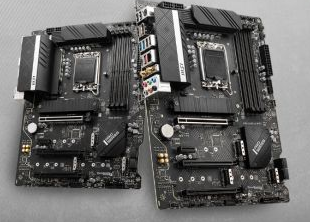
According to the number of circuit boards, circuit boards are divided into three categories: single-sided, double-sided and multilayer circuit boards.
First, the single board is concentrated on one of the leads of the most basic PCB part. Because the wires only appear on one of the sides, it is called a single-sided circuit board. Single-sided boards are usually simple and low-cost, but the disadvantage is that they cannot be applied to overly complex products.

The double-sided board is an extension of the single-sided board. When single-layer cables cannot meet the needs of electronic products, double-sided panels must be used. Both sides are covered with copper wires, and two layers of wires can be introduced through the holes to form the required network connection.
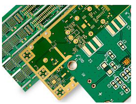
Multi-layer board refers to the mutual compression of more than three conductive pattern layers and the insulating material between them, and the conductive patterns need to be connected. Multilayer circuit boards are the product of the development of electronic information technology in the direction of high-speed, multi-function, large-capacity, small volume, thinness and light weight...
Circuit boards are divided into flexible boards (FPC), rigid boards (PCB), and rigid-flex boards (FPCB) according to their characteristics.
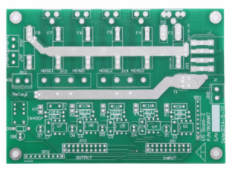
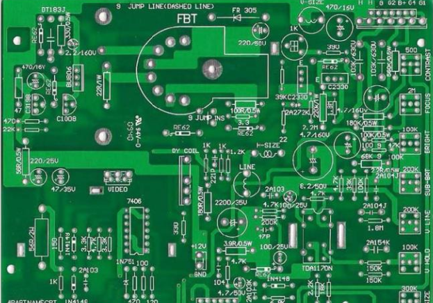
The two sides of the PCB board are the top and the bottom. This is a double-layer circuit board. The double-layer circuit board is a double-sided copper-plated PCB board. The double-layer circuit boards are covered with copper and wires, and two layers of wires can be introduced through the holes to form the required network connection.
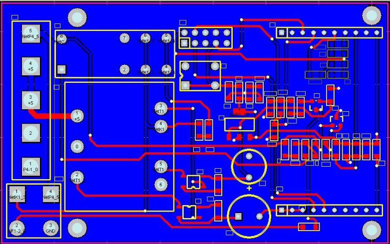
Prepare circuit schematics..
2. Create a new PCB file and package it into the component packaging library.
Planning the circuit board 3..
4 is included in the netlist and components.
Automatic layout of 5 yuan equipment.
Adjust the layout 6.
Network density analysis 7..
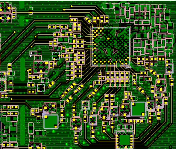
Wiring rule settings.
9 automatic wiring.
10 Manually adjust the line.
Commonly used EDA circuit software can design multi-layer PCB circuit boards. Although the methods are different, the principles are the same.
PCB design AD provides 10 different design rules. These design rules include rules such as wire placement, wire placement, component placement, routing rules, component movement, and signal integrity. According to these rules, ProtelDXP is automatic layout and automatic routing. To a large extent, the success of the cable and the quality of the cable depend on the rationality of the design rules and the design experience of the user.
For specific circuits, different design rules can be used. If a double panel is designed, you can use the default value system of the system to set the double panel.
Here, I want to share a four-layer PCB setup steps, 8-layer boards and other multi-layer boards are set up like this. Other versions of ads are similar to this operation.
First, if you have your own project, you can create a new PCB file in your own project.
Choose File-New-PCB.
As you can see, the built PCB has only two layers of Tople and Portum games. As shown below.
Open layer management. Enter the cascade management interface.
As you can see, there are currently only two-story Rangers and Potham Rangers. You can see an advertising option on the right. After the modification, we can see that the four-layer PCB board has been set up to increase the GND and VCC layers. By introducing the compiled schematic diagram, the PCB diagram of the four-layer board can be drawn.
The operation skills of each floor are the same as the single panel, and only need to be fully considered in the design.
First, if you have your own project, you can create a new PCB file in your own project.
Choose File-New-PCB.
2. As you can see, the built PCB has only two layers, TopLayer and BottomLayer. As shown below.
Open layer management. Enter the cascade management interface.
As you can see, there are currently only two-story Rangers and Potham Rangers. You can see an advertising option on the right. After the modification, we can see that the four-layer PCB board has been set up to increase the GND and VCC layers. By introducing the compiled schematic diagram, the PCB diagram of the four-layer board can be drawn.