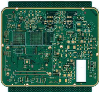
PCB companies commonly used circuit board processing processes are as follows: Single-panel process, double-panel process, multi-layer board process, PCB material selection, PCB material selection a) The substrate with higher Tg should be selected appropriately-glass transition temperature Tg is a characteristic property of polymers, a critical temperature that determines material properties, and a key parameter for selecting substrates. The Tg of epoxy resin is around 125~140 degree Celsius, and the reflow soldering temperature is around 220 degree Celsius, which is much higher than the Tg of PCB substrate. High temperature can easily cause thermal deformation of PCB and damage components in severe cases. *Tg should be higher than the working temperature of the circuit. b) Low CTE is required-due to the inconsistency of the thermal expansion coefficients in the X, Y and thickness directions, it is easy to cause PCB deformation, and in severe cases, the metallized holes will break and components will be damaged. c) High heat resistance is required-generally the PCB is required to have a heat resistance of 250°C/50S. d) Good flatness is required. e) Electrical performance requirements: materials with low dielectric constant and low dielectric loss are required for high-frequency circuits. Insulation resistance, withstand voltage strength, and arc resistance must meet product requirements.

PCB thickness design 1. Allowable board thickness for general placement machines: 0.5~5mm. 2. The thickness of PCB is generally in the range of 0.5~2mm. 3. Assemble only low-power components such as integrated circuits, low-power transistors, resistors, capacitors, etc., under the condition of no strong load vibration, use a thickness of 1.6mm, and the size of the board within 500mm*500mm; 4. Yes Under load vibration conditions, it is necessary to reduce the size of the plate or strengthen and increase the support points according to the vibration conditions, and the 1.6mm plate can still be used; 5. When the plate surface is large or cannot be supported, consider increasing the plate thickness. Should choose 2~3mm thick board. 6. When the level is higher, the thickness of each layer must be ensured to meet other requirements (such as withstand voltage requirements). 7. When the PCB size is smaller than the minimum mounting size, the boarding method must be used. Design of laminated structure In the design of laminated structure, we are committed to the design and production of laminated structure that meets the needs of customers. The basic design principles are as follows: When the customer has a specified structure, it must be designed according to customer requirements. When the customer has impedance requirements, a laminate structure that meets the customer's requirements must be used. When the customer does not specify the structure, the design principle is: the thickness of the dielectric layer and the pressing thickness meet the customer's requirements. The inner layer is preferentially selected with a thicker core plate; the minimum dielectric thickness: 0.06mm, as far as possible, use a single PP structure. The surface PP can only discharge 1080, 2116 laminate structure design software. Misunderstanding of laminate structure caused by the Protel series software design PCB file has a description of the media thickness requirement, as shown in the right picture, if the layer is obtained without special settings The pressure structure is equal to the medium. Then the thickness of the core board becomes smaller, the quantity of PP increases, and the cost increases. If there is no requirement, it is recommended to specify in the processing requirements. Inner graphic design Inner graphic design The distance between the inner hole and the line should be increased as much as possible, the higher the level, the greater the distance. (4 layer boards are guaranteed to be more than 7mil, 6-8 layers are guaranteed to be more than 8mil) The higher the level, the greater the distance between the inner hole and the copper, generally more than 10MIL, which improves the reliability. In areas with dense holes, the line should be placed in the middle of the two holes as much as possible. The elements in the board are more than 15 mils away from the edge of the board. The higher the level, you can consider increasing it. Spread copper under the golden fingers to prevent the area from being thin. Frequently Asked Questions-The inner network is not clear. A) The hole is tangent to the inner graph, and the network cannot be judged. B) The hole design is on the isolation line, and the PAD design of the hole location is incomplete, and the network cannot be determined. C) The quincunx pad is designed on the isolated line, and its network cannot be determined. Drilling design Drilling design 4) Thickness-to-diameter ratio: The ratio of hole to plate thickness is preferred: less than 1:8, and it is difficult to process when 1:8 or more. 5) When using the reflow soldering process, the via hole setting A. Generally, the via hole diameter is not less than 0.3mm; the ratio of the minimum hole diameter to the board thickness is not less than 1:8. If the ratio is too small, the process will be more difficult when the hole is metalized. Rising costs. B. The via hole cannot be directly set on the pad, the extension of the pad and the corner of the pad. C. There should be a thin wire coated with solder mask between the via and the pad. The length of the thin wire should be greater than 0.5mm and the width greater than 0.1mm. Drilling design 6) The minimum hole diameter is 0.2MM. Large holes can be used as much as possible. The distance between the edge of the hole and the edge of the hole is greater than 12mil, and the via hole should not be drilled on the pad that needs to be soldered. 7) PCB aperture tolerance control range: The normal aperture tolerance is in accordance with the IPC 2 standard. The tolerance of the crimp hole diameter can be controlled within ±0.05mm. PTH can control the hole diameter tolerance ±0.08mm. NTPH can control the hole diameter tolerance ±0.05mm. 8) Hole position tolerance ±0.075mm 9) Hole copper requirements: IPC 3 standard control Hole copper average 25um, single point greater than 20um. The most common problems of drilling files communicate the design of the outer circuit 1. Limit line width spacing 3/3MIL, usually finished product 1OZ minimum line width/spacing 4.5/4.5MIL, finished product 2OZ minimum line width/spacing 6/6MIL, subsequent increase The copper thickness is 1OZ, and the line width and spacing are correspondingly increased by 1MIL, corresponding to the copper thickness of the inner layer line width and spacing. Circumstances allow it to be recommended to increase 1MIL separately. 2. The current-carrying capacity of the line width at different temperatures (1OZ). Line width current-carrying capacity comparison table Outer layer circuit design 3. Teardrops should be added to the PCB pad trace to avoid the pad being pulled off during wave soldering. 4. No vias can be placed on the SMD pads, and the vias and pads should be kept 0.2m away.