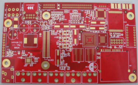
PCB circuit board and pattern (Pattern): The circuit is used as a tool for conduction between the originals. In the design, a large copper surface will be additionally designed as a ground and power layer. The route and the drawing are made at the same time.
Dielectric layer (Dielectric): Used to maintain the insulation between the circuit and each layer, commonly known as the substrate.
Hole (Through hole / via): The through hole can make the lines of more than two levels connect to each other. The larger through hole is used as a part plug-in. In addition, there are non-through holes (nPTH) that are usually used as surface mounts. It is used for fixing screws during assembly.
Solder resistant /Solder Mask: Not all copper surfaces need to be tin-on parts, so the non-tin area will be printed with a layer of substance (usually epoxy resin) that insulates the copper surface from eating tin. Short circuits between non-tinned circuits.
Silk screen (Legend /Marking/Silk screen): This is a non-essential structure. The main function is to mark the name and position frame of each part on the circuit board, which is convenient for maintenance and identification after assembly.
Surface Finish: Because the copper surface is easily oxidized in the general environment, it can not be tinned (poor solderability), so it will be protected on the copper surface that needs to be tinned.
The methods of protection include HASL, ENIG, Immersion Silver, Immersion Tin, and Organic Solder Preservative (OSP). Each method has its advantages and disadvantages, which are collectively referred to as surface treatment.
What are the advantages of PCB multilayer boards
The biggest difference between a multi-layer board and a single-sided board and a double-sided board is the addition of an internal power layer (to maintain the internal electrical layer) and a ground layer. The power supply and ground wire network are mainly wired on the power layer.

However, multi-layer board wiring is mainly based on the top and bottom layers, supplemented by the middle wiring layer. Therefore, the design of the multi-layer board is basically the same as the design method of the double-sided board. The key is how to optimize the wiring of the inner electrical layer, so that the wiring of the circuit board is more reasonable and the electromagnetic compatibility is better.
How to imitate PCB boards and circuit boards
PCB copy board is usually called PCB imitation or PCB cloning. Simply put, it is to copy and clone the same or similar PCB board through electronic products. The whole process of copying PCB board requires certain technology and process operation method.
PCB copy board is a reverse engineering of PCB design. It first removes the components on the PCB circuit board to make a BOM list, scans the empty board into a picture and restores it to a PCB board drawing file through the copying software; the PCB board drawing file Send it to the PCB factory to make the board (PCBA), and then add the components (purchase the corresponding components according to the BOM list), which is exactly the same PCB circuit board as the original PCB circuit board.
1. After getting a PCB, first record the model, parameters, and positions of all vital parts on the paper, especially the direction of the diode, the tertiary tube, and the direction of the IC gap. It is best to use a digital camera to take two photos of the location of the vital parts. The current PCB circuit boards are getting more and more advanced. Some of the diode transistors above are not noticed at all.
2. Remove all components and remove the tin in the PAD hole. Clean the PCB with alcohol and put it into the scanner. When the scanner scans, you need to raise the scanned pixels slightly to get a clearer image. Then lightly polish the top and bottom layers with water gauze until the copper film is shiny, put them in the scanner, start PHOTOSHOP, and scan the two layers in separately in color. Note that the PCB must be placed horizontally and vertically in the scanner, otherwise the scanned image cannot be used.
3. Adjust the contrast and brightness of the canvas to make the part with copper film and the part without copper film have a strong contrast, then turn the second image into black and white, and check whether the lines are clear. If not, repeat this step. If it is clear, save the picture as black and white BMP format files TOP.BMP and BOT.BMP. If you find any problems with the graphics, you can also use PHOTOSHOP to repair and correct them.
4. Convert the two BMP format files to PROTEL format files, and transfer to two layers in PROTEL. For example, the positions of PAD and VIA that have passed through two layers basically coincide, indicating that the previous steps have been done well. If there is a deviation, Then repeat the third step. Therefore, PCB copying is a work that requires patience, because a small problem will affect the quality and the degree of matching after copying.