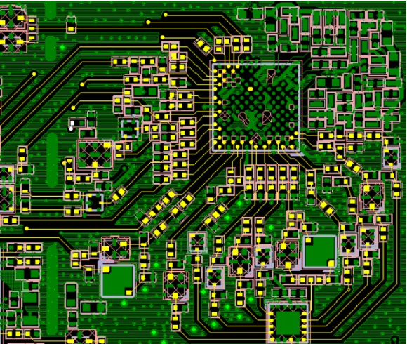
Almost all the FPC manufacturing processes so far have been processed by the subtractive method (etching method). Usually, a copper clad board is used as a starting material, a resist layer is formed by photolithography, and the unnecessary part of the copper surface is etched and removed to form a circuit conductor. Due to problems such as undercutting, the etching method has limitations in the processing of fine circuits.
Based on the processing difficulties of the subtractive method or the difficulty in maintaining high-yield microcircuits, the semi-additive method is considered to be an effective method, and various semi-additive methods have been proposed. An example of micro-circuit processing using the semi-additive method. The semi-additive process starts with a polyimide film, and first casts (coats) a liquid polyimide resin on a suitable carrier to form a polyimide film.
Next, a sputtering method is used to form a seeding layer on the polyimide base film, and then a resist pattern of the reverse pattern of the circuit is formed on the seeding layer by photolithography, which is called a plating resistant layer.

The blank part is electroplated to form a conductor circuit. Then remove the resist layer and unnecessary seeding layer to form the first layer of circuit. Coating photosensitive polyimide resin on the first layer of circuits, using photolithography to form holes, protective layers or insulating layers for the second circuit layer, and then sputtering on them to form a seeding layer, as The base conductive layer of the second layer of the circuit. By repeating the above process, a multilayer circuit can be formed.
Using this semi-additive method, ultra-fine circuits with a pitch of 5um and a via hole of 10um can be processed. The key to the production of ultra-fine circuits using the semi-additive method is the performance of the photosensitive polyimide resin used as the insulating layer.
Composing material
1. Insulating film
The insulating film forms the base layer of the circuit, and the adhesive bonds the copper foil to the insulating layer. In a multi-layer design, it is then bonded to the inner layer. They are also used as a protective cover to insulate the circuit from dust and moisture and to reduce stress during flexing. The copper foil forms a conductive layer.
In some flexible circuits, rigid components made of aluminum or stainless steel are used, which can provide dimensional stability, physical support for the placement of components and wires, and stress relief. The adhesive bonds the rigid component and the flexible circuit together. In addition, there is another material sometimes used in flexible circuits, which is the adhesive layer, which is formed by coating the two sides of the insulating film with an adhesive. The adhesive layer provides environmental protection and electrical insulation functions, and can eliminate a layer of film, and has the ability to bond multiple layers with a small number of layers.
2. Conductor
Copper foil is suitable for use in flexible circuits. It can be electrodeposited (ED) or plated. One side of the electrodeposited copper foil has a glossy surface, while the processed surface on the other side is dull and dull. It is a flexible material that can be made into many thicknesses and widths. The matte side of ED copper foil is often specially treated to improve its bonding ability. In addition to flexibility, forged copper foil also has the characteristics of rigidity and smoothness. It is suitable for applications that require dynamic deflection.
3. Adhesive
In addition to bonding the insulating film to the conductive material, the adhesive can also be used as a covering layer, as a protective coating, and as a covering coating. The main difference between the two lies in the application method used. The cover layer is bonded to the cover insulating film to form a circuit with a laminated structure. Screen printing technology used for covering and coating of adhesive.
Not all laminate structures contain adhesives, and laminates without adhesives form thinner circuits and greater flexibility. Compared with the laminated structure based on adhesive, it has better thermal conductivity. Due to the thin structure of the adhesive-free flexible circuit and the elimination of the thermal resistance of the adhesive, thereby improving the thermal conductivity, it can be used in a working environment where the flexible circuit based on the adhesive laminated structure cannot be used. .
basic structure
Copper foil substrate: CopperFilm. Copper foil: basically divided into electrolytic copper and rolled copper, the common thickness is 1oz, 1/2oz and 1/3oz. Substrate film: There are two common thicknesses: 1mil and 1/2mil. Glue: Adhesive, the thickness is determined according to customer requirements. Cover film protection film: CoverFilm, used for surface insulation, common thicknesses are 1mil and 1/2mil. Release paper: It is easy to work to prevent the adhesive from sticking to foreign matter before pressing. Reinforcement board: PIStiffenerFilm, which reinforces the mechanical strength of the FPC and facilitates surface mounting operations. The common thickness is 3mil to 9mil. EMI: Electromagnetic shielding film to protect the circuit inside the circuit board from outside interference (strong electromagnetic area or susceptible to interference area).