The development of today's technology and industry has brought about tremendous changes in social life. We have noticed that with the gradual popularization of the Internet of Things, big data, and AI intelligent applications, the development and application requirements of PCB drilling have undergone tremendous changes. The editor will take you to understand what factors should be considered for PCB drilling.
1. The equipment factor Spindle Runout is too large and the presser foot is worn unevenly, which causes crushing damage to the aluminum sheet during drilling, and affects the dust collection effect. In severe cases, a large amount of drill chips may be seen under the aluminum sheet, and the dust suction strength is too low.
2. There are serious scratches or creases on the aluminum sheet of the cover and bottom plate, and the drill bit, especially the Microdrill drill, may break the drill bit at these defects. The bottom material is poor and contains impurities. The size of the aluminum sheet is too large, and the aluminum sheet is arched after the adhesive tape is applied, which causes increased wear of the presser foot and poor dust collection effect. The size of the aluminum sheet is too small, and the hole is drilled on the edge of the aluminum sheet or tape.

3. Operating factors During the board loading process, the work surface (pad board), the bottom board, the production board and the cover board are poorly cleaned, and the drill bit is drilled on the debris and the drill bit is broken. The drilling depth is too deep, causing deterioration of chip removal conditions during drilling.
4. Drilling nozzle control The cutting length of the drill nozzle is too short, resulting in poor chip removal. Too many regrind times of the drill tip result in too short effective cutting length of the drill tip, excessive drill tip wear, and reduced chip removal level. The drill bit control (including the drill bit pick-up, ringset making and grinding) is not good.
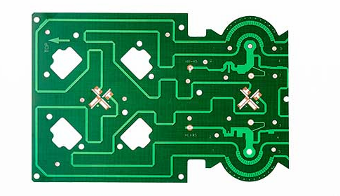
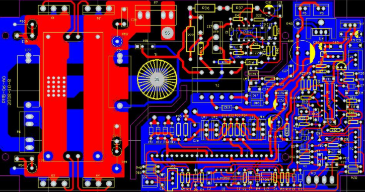
The PCB drilling process refers to stacking several printed boards together, and drilling with the above completed hole size at the same time. The above drill size 9 (depending on the plating requirements) is mainly considering that a certain amount of plating metal will flow into the hole. Holes that are completely drilled with copper, and holes that are not plated will be plated in the environment below.
PCB manufacturers limit the minimum use size of drilling holes according to the thickness of the printed board. The rule is that the thinner the printed board, the smaller the cutter head of the drilling machine. The expression of this data is the plate thickness-to-aperture ratio, including the rough-machined plate thickness-to-aperture ratio and the finished plate thickness-to-aperture ratio. The rough-machined plate thickness-to-aperture ratio refers to the size of the actual drilled hole, and the finished plate thickness-to-aperture ratio refers to the size after standard electroplating is included. The manufacturer shall refer to the actual drilling size, and the designer shall refer to the completed hole size. The designer must determine whether the data he refers to is the ratio of thickness to aperture for rough machining or the ratio of thickness to aperture for finished plate. The board thickness-to-aperture ratio is limited by the smallest drilling machine. Therefore, no matter how small the data of the board thickness-to-aperture ratio is, it cannot be updated with the completed smallest drilling machine. The terms roughing and finishing are always clearly discussing drilling Used when the hole size and the plate thickness hole ratio are used. The thickness-to-aperture ratio is always based on the printed board before electroplating.
Secondary drilling: When the hole is located on the copper area but should not be electroplated, a secondary drilling is required. The land around the unplated hole is the so-called unsupported land. PCB electroplating can prevent the pad from deforming, dissipate heat from the pad, and prevent solder bumps during soldering. Such holes increase the electroplating process, which will increase the overall cost. There are two ways to electroplate all pairs of holes, or to reserve a certain "clean area" around the hole and the copper area to eliminate secondary drilling.