1. Backing board for PCB drilling
Phenolic resin laminated board, used as a backing board for PCB drilling and bakelite board for insulation and mold fixtures. The backing board and the bakelite board have the same characteristics of high temperature resistance and resistance to deformation, high flatness, and can be used in high-end PCB drilling technology. Compressed by pressing machine, it is a plate-like laminated product. Among them, the main products of the backing board department are divided into upper cover and lower backing board. The former types include pure aluminum, soft and hard aluminum alloy, bakelite and LE series; the latter includes melamine-covered phenolic board, phenolic resin board, melamine-covered wood pulp board, wood pulp board, etc.
The purpose of the upper cover plate is to protect the board surface when drilling the PCB; at the same time, fix the drill pin to reduce the offset; prevent the substrate from burrs; assist the drill pin to spread the fever and help to clean the hole of the drill pin.

Under the above-mentioned purpose, the upper cover plate also has five major requirements, including sufficient softness, excellent thickness tolerance, flatness, high temperature resistance, and low moisture absorption and resistance to deformation.
As for the use of the lower backing plate, it is to suppress the hair, run through the PCB board, protect the drilling machine and ensure the quality of the substrate. Its characteristic requirements are good flatness, excellent dimensional tolerance, easy cutting, hard and flat surface, and high temperature material. Do not produce stickiness or release chemical substances to contaminate the hole wall or drill needle, and the drill cuttings must be soft so as not to scratch the hole wall.
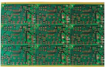
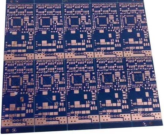
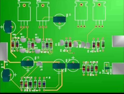
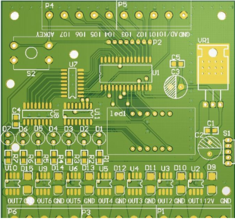
2. BGA processing skills of PCB copy board technology
One, the production of the outer circuit BGA:
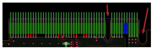
Before processing the customer data, first fully understand the specifications of the BGA, the size of the customer's design pad, the array situation, the size of the via under the BGA, and the distance between the hole and the BGA pad. The copper thickness is required to be 1~ For 1.5-ounce PCB boards, except for specific customer’s production according to their acceptance requirements, the compensation is generally 2mil if the mask etching process is used in the production, and 2.5mil is compensated if the electrical process is used, and the specification is 31.5mil BGA Do not use electrical graphics processing; when the customer designed the BGA to the via hole spacing is less than 8.5mil, and the BGA under the via hole is not centered, the following methods can be used:
You can make a standard BGA array according to the BGA specification and design pad size corresponding to the BGA position designed by the customer, and then take the BGA and BGA lower vias that need to be calibrated based on it, and back it up with the original before. Check the effect of the front and back of the shot. If the deviation between the front and rear of the BGA pad is large, it cannot be used. Only the location of the via under the BGA is shot.
2. BGA solder mask production:
1. BGA surface mount solder mask opening: the same as the solder mask optimization value, its unilateral opening range is 1.25~3mil, and the solder mask line (or via pad) spacing is greater than 1.5mil;
2, BGA corresponding hole blocking layer, character layer processing:
1. Where plugging is needed, no blocking points are added on both sides of the plugging layer;
2. The via hole at the character layer opposite to the plug hole allows white oil to enter the hole.
Three, BGA plug hole template layer and backing layer processing:
1. Make the 2MM layer: copy the PCB circuit layer BGA pad into another 2MM layer and treat it as a square with a 2MM range. There must be no vacancies or gaps in the middle of the 2MM (if there are customer requirements, use the character frame at the BGA as For the range of the plug hole, the character frame at the BGA is the 2MM range for the same treatment). After making the 2MM entity, compare it with the character frame at the BGA of the character layer. The larger of the two is the 2MM layer.
2. The plugging layer (JOB.bga): Touch the 2MM layer with the hole layer (use the Actionsàreference selection function in the panel to refer to the 2MM layer for selection), select Touch for the parameter Mode, and copy the holes to be plugged within the BGA 2MM range to the plugging layer, and Name it: JOB.bga (note that if the customer requires that the test hole at the BGA is not plugged, the test hole must be selected. The feature of the BGA test hole is: full window on both sides of the solder mask or window on one side).
3. Copy the plug hole layer to another backing layer (JOB.sdb).
4. Adjust the hole diameter of the plug hole layer and the backing plate layer according to the BGA plug hole file.