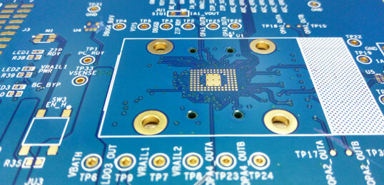
Multi-layer PCB stack structure
Before designing a multilayer printed circuit board, the designer must determine the structure of the circuit board (CEM) according to the size of the circuit, the size of the printed circuit board and the electromagnetic compatibility requirements, that is, the use of 4, 6 or more circuit boards.
Circuit board. Determine the number of layers, determine the location of internal layers, and determine how to distribute different signals on these layers. This is the choice of PCB cascade structure.
The cascade structure is an important factor that affects the CEM performance of the printed circuit board, and is also an important means of suppressing electromagnetic interference. This section introduces the relevant content of the multilayer laminate structure of PCBs.
1.1. Principles for the selection of layers and stacks Many factors must be considered when determining the laminate structure of the PCB multilayer board.
In terms of PCB wiring, more layers are high, and the best is wiring, but the cost and difficulty of the card will increase.
For PCB manufacturers, in the manufacturing process of printed circuit boards, the symmetry of the stacked structure has been extensively analyzed. Therefore, the selection of each layer must consider all aspects required to achieve the greatest balance.
For experienced designers, after the component is preset, the printed circuit routing bottleneck will be analyzed and combined with other EDA tools to analyze the cable density of the printed circuit, followed by the number and type of signal lines with special wiring requirements.
When determining the number of signal layers, composite such as differential lines and sensitive signal lines, and then determine the number of inner layers according to the type of power supply, isolation requirements and interference protection.
In this way, the number of layers of the circuit board is basically determined. After determining the number of layers of the printed circuit board, the next task is to rationally arrange the order of placement of the circuit layers.
At this stage, two main factors must be considered.

(1) The allocation of special signal layer.
(2) The distribution of food and grassland. There are more printed circuit layers, including special signal layers, layers and power layers.
It is more difficult to determine which combination is the best, but the general principles are as follows.
(1) The signal layer should be adjacent to the inner layer (power/internal formation), and the main copper film of the inner layer should be used to protect the signal layer.
There must be a narrow coupling between the internal power supply layer and the layer, that is, the average thickness between the internal power supply layer and the layer must be a lower value to improve the ability between the power supply layer and the layer and increase the resonance frequency.
The internal power layer and the dielectric thickness between the layers can be defined in the proton stack manager (layer stack manager). Command, system level management dialog box, double-click the text pre-extracted with the mouse pointer.
1. Insulation layer in the fold option of the dialog box. If the potential difference between the power supply and ground is not important, you can use a lower insulation thickness, such as 5 ml (0.127 mm).
(3) The high-speed signal transmission layer in the circuit should be the middle layer of the signal and interfere between the two inner layers. Therefore, the copper films of the two inner layers can be electromagnetic shields for high-speed signal transmission, and can effectively limit the radiation of high-speed signals between the two inner layers without causing external interference.
(4) Open the two directly adjacent signal layers. It is easy to perform crosstalk between adjacent signal layers, resulting in circuit failure. By adding a quality plane between the two signal layers, crosstalk can be effectively prevented.
(5) Some land use layers can effectively resist the land. For example, the common mode interference can be effectively reduced by using different quality plans in the A and B signal layers. Consider the symmetry of the layered structure.
1.2 Common cascade structure The following is an example of four layers to illustrate how to optimize the arrangement and combination of different cascade structures. On a four-layer fluent four-layer board, there are several different stacking modes (up and down).
So, how do we choose between the first plan and the second plan? Generally speaking, the designer will choose Figure 1 as the structure of the four-layer board.
But the common printed circuit board only places the components on the upper layer. Therefore, it is best to use frame 1. However, when the upper and lower layers must put the thickness between the components and the internal power layer and this layer between the larger layers, and the coupling is not good, at least one signal line layer must be considered.
There are fewer signal lines in the lower layer, and a large copper surface can be used to couple the power layer.
On the contrary, if the part is mainly located in the lower layer, in order to realize the map. Then the power layer is coupled with the yarn layer itself.
Taking into account the requirement of symmetry, Outline 1 is generally accepted. After completing the analysis of the four-layer laminate structure, an example of the six-layer laminate structure is provided to illustrate the combined device and method as well as the method of optimizing the six-layer laminate structure.
In all respects, Figure 3 is clearly the best, and Figure 3 is also a regular cascade structure of six-layer laminates. When analyzing the above two examples, I think that readers have a certain understanding of the cascade structure, but in some cases, a system cannot meet all the requirements, which requires consideration of the priority of design principles.
Unfortunately, because the design of PCBs is related to the characteristics of the updated circuit.
The firewall performance and design appearance of different circuits are different, so in fact, these principles do not have the ultimate reference value.
However, this must be the design principle 2 (internal power layer and layer should) should be satisfied in the first design.
In addition, high-speed signals need to be carried out in the circuit, and then design principle 3 (the high-speed signal transmission layer in the circuit should be the signal interlayer in the middle layer, and the sandwich between the two inland) must be satisfied.
iPCB is a high-tech manufacturing enterprise focusing on the development and production of high-precision PCBs. iPCB is happy to be your business partner. Our business goal is to become the most professional prototyping PCB manufacturer in the world. Mainly focus on microwave high frequency PCB, high frequency mixed pressure, ultra-high multi-layer IC testing, from 1+ to 6+ HDI, Anylayer HDI, IC Substrate, IC test board, rigid flexible PCB, ordinary multi-layer FR4 PCB, etc. Products are widely used in industry 4.0, communications, industrial control, digital, power, computers, automobiles, medical, aerospace, instrumentation, Internet of Things and other fields.