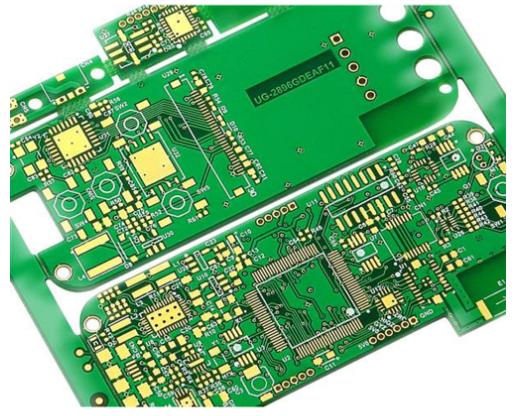
For PCB design, you have to know these 15 principles, and I hope it will be helpful to everyone.
1. The PCB clock frequency exceeds 5MHZ or the signal rise time is less than 5ns, generally a multilayer board design is required. The signal loop area can be well controlled by adopting multi-layer board design.
2. For multi-layer boards, the key wiring layer (the layer where the clock line, bus, interface signal line, radio frequency line, reset signal line, chip select signal line and various control signal lines are located) should be adjacent to the complete ground plane, preferably Between two ground planes.
Key signal lines are generally strong radiation or extremely sensitive signal lines. Wiring close to the ground plane can reduce the signal loop area, reduce its radiation intensity or improve anti-interference ability.
3. For single-layer boards, both sides of key signal lines should be covered with ground. The key signal is wrapped with ground on both sides, on the one hand, it can reduce the area of the signal loop, and on the other hand, it can prevent the crosstalk between the signal line and other signal lines.
4. For the double-layer board, the projection plane of the key signal line has a large area of ground, or the ground is punched like a single board. It is the same as the key signal of the multilayer board is close to the ground plane.

5. In a multilayer board, the power plane should be retracted by 5H-20H relative to its adjacent ground plane (H is the distance between the power supply and the ground plane). The retraction of the power plane relative to its return ground plane can effectively suppress the edge radiation problem.
6. The projection plane of the wiring layer should be in the area of the reflow plane layer. If the wiring layer is not in the projection area of the reflow plane layer, it will cause edge radiation problems and increase the area of the signal loop, resulting in an increase in differential mode radiation.
7. In the multi-layer board, the TOP and BOTTOM layers of the single board should not have signal lines larger than 50MHZ as much as possible. It is best to walk the high-frequency signal between the two plane layers to suppress its radiation to the space.
8. For single boards with board-level operating frequencies greater than 50MHz, if the second layer and the penultimate layer are wiring layers, the TOP and BOOTTOM layers should be covered with grounded copper foil. It is best to walk the high-frequency signal between the two plane layers to suppress its radiation to the space.
9. In a multi-layer board, the main working power plane of the single board (the most widely used power plane) should be in close proximity to its ground plane. The adjacent power plane and ground plane can effectively reduce the loop area of the power circuit.
10. In a single-layer board, there must be a ground wire next to and parallel to the power trace. Reduce the power supply current loop area.
11. In a double-layer board, there must be a ground wire next to and parallel to the power trace. Reduce the power supply current loop area.
12. In the layered design, try to avoid the arrangement of adjacent wiring layers. If it is unavoidable that the wiring layers are adjacent to each other, the layer spacing between the two wiring layers should be appropriately increased, and the layer spacing between the wiring layer and its signal circuit should be reduced. Parallel signal traces on adjacent wiring layers can cause signal crosstalk.
13. Adjacent plane layers should avoid overlapping of their projection planes. When the projections overlap, the coupling capacitance between the layers will cause the noise between the layers to couple with each other.
14. When designing the PCB layout, fully comply with the design principle of placing in a straight line along the signal flow direction, and try to avoid looping back and forth. Avoid direct signal coupling and affect signal quality.
15. When multiple module circuits are placed on the same PCB, digital circuits and analog circuits, and high-speed and low-speed circuits should be laid out separately. Avoid mutual interference between digital circuits, analog circuits, high-speed circuits, and low-speed circuits.