1. Basic principles of power supply wiring and power supply bypass
When designing an RF circuit, the design of the power supply circuit and the PCB layout are often left until the design of the high-frequency signal path is completed. For a design that has not been carefully thought out, the power supply voltage around the circuit is prone to erroneous output and noise, which will negatively affect the system performance of the RF circuit. Properly assigning PCB layers, using star-shaped VCC leads, and adding appropriate decoupling capacitors to the VCC pin will help improve the performance of the system and obtain the best indicators.
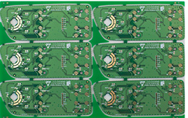
Reasonable PCB layer allocation is convenient to simplify subsequent wiring processing. For a four-layer PCB (a commonly used circuit board in WLAN), in most applications, the top layer of the circuit board is used to place components and RF leads, and the second layer is used as the system ground. The power part is placed on the third layer, and any signal lines can be distributed on the fourth layer.
The combination of good power supply decoupling technology with rigorous PCB layout and VCC leads (star topology) can lay a solid foundation for any RF system design. Although there will be other factors that reduce system performance indicators in the actual design, having a "noise-free" power supply is the basic element for optimizing system performance.

2. The basic principles of RF grounding and via design
The layout and lead of the ground are also the key to the design of the WLAN circuit board, they will directly affect the parasitic parameters of the circuit board, and there is a hidden danger of reducing the performance of the system. There is no unique grounding scheme in RF circuit design. There are several ways to achieve satisfactory performance indicators in the design. The ground plane or lead can be divided into analog signal ground and digital signal ground, and it can also isolate circuits with high current or high power consumption.
After the ground plane is determined, connect all signal grounds to the ground plane with the shortest path. Usually vias are used to connect the ground wire of the top layer to the ground plane. It should be noted that the vias are inductive.
Filter out the noise of other circuits and suppress the noise generated locally, thereby eliminating the cross interference between the stages through the power line, which is the benefit of VCC decoupling. If the decoupling capacitor uses the same ground via, due to the inductance effect between the via and the ground, the vias at these connection points will carry all the RF interference from the two power supplies, which not only loses the function of the decoupling capacitor, but also It also provides another path for the inter-stage noise coupling in the system.
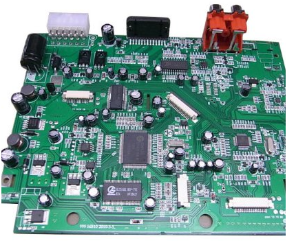
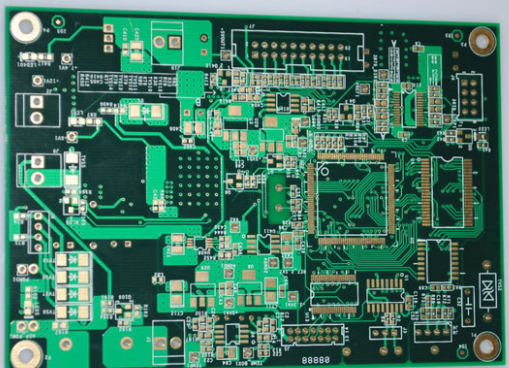
Figure 6 shows an example of PCB layout. There are many ground vias on the ground pad.
3. Suppress PLL spurious signals through proper power supply bypass and grounding
It is a difficult point in the design process to meet the requirements of the 802.11a/b/g system to transmit the spectrum mask. The linearity index and power consumption must be balanced, and a certain margin must be reserved to ensure that it meets the IEEE under the premise of maintaining sufficient transmit power. And FCC regulations. The typical output power required by the IEEE 802.11g system at the antenna end is +15dBm, and the frequency deviation is -28dBr when the frequency deviation is 20MHz. The power rejection ratio (ACPR) of adjacent channels in a frequency band is a function of the linear characteristics of the device, which is correct for a specific application under certain premises. A large amount of work to optimize the ACPR characteristics in the transmission channel is achieved by adjusting the bias of the Tx IC and PA based on experience, and tuning the matching network of the input stage, output stage and intermediate stage of the PA.
In addition, if the power supply wiring is unreasonable, for example, the power lead of the VCO is located just below the charge pump power supply, the same noise can be observed on the VCO power supply, and the generated spurious signals are enough to affect the ACPR characteristics, even if the decoupling is strengthened, the test The result will not be improved. In this case, it is necessary to examine the PCB wiring and rearrange the power supply leads of the VCO, which will effectively improve the stray characteristics and meet the specifications required by the specification.