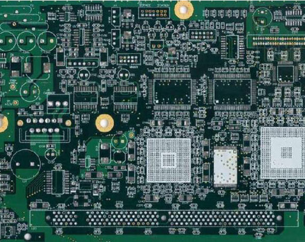
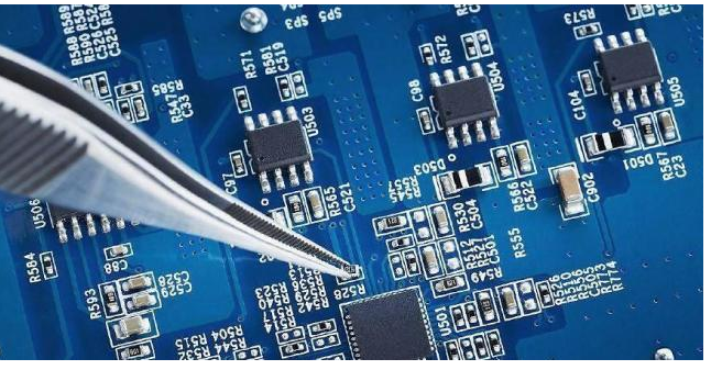
This article introduces the ten most effective design rules that electronic design engineers should keep in mind and practice when using design software for printed circuit board layout design and commercial manufacturing. Engineers do not need to implement these rules in order based on time or relative importance, just follow them to greatly change the product design.
Rule 1: Choose the correct grid set and always use grid spacing that matches most components. Although multigrid seems to be effective, if engineers can think more in the early stages of printed circuit board layout design, they can avoid pitch difficulties and maximize the use of circuit boards. Since many devices have multiple packaging sizes, engineers should use the product that is most conducive to their own design. In addition, polygons are very important for copper plating on circuit boards. When multi-grid circuit boards are copper-plated on polygons, polygon filling deviations usually occur. Although it is not based on a single grid standard, it can provide a longer life than the required circuit board life.

Rule 2: Keep the path shortest and direct. This sounds simple and common, but it should be kept in mind at every stage, even if it means changing the board layout to optimize the wiring length. This applies especially to analog and high-speed digital circuits, where system performance is always partially limited by impedance and parasitic effects.
Rule 3: Use the power layer as much as possible to manage the distribution of power and ground. For most PCB board design software, the copper coating on the power layer is a faster and simpler choice. By connecting a large number of wires together, the current with the highest efficiency and the lowest impedance or voltage drop can be ensured, and at the same time, sufficient ground loops can be provided. If possible, you can also run multiple power lines in the same area of the circuit board to confirm whether the ground layer covers most layers of the printed circuit board, which facilitates the interaction between the running lines on adjacent layers.
Rule 4: Use required test points to group related components. For example, the discrete components required by OpAmp operational amplifiers are placed close to the device so that bypass capacitors and resistors can be matched with the same ground, which helps to optimize what is mentioned in Rule 2. The wiring length makes testing and fault detection easier at the same time.
Rule 5: Repeat the required circuit board on another larger circuit board. Carry out the printed circuit board layout multiple times. Choosing the most suitable size for the equipment used by the manufacturer can help reduce prototyping and manufacturing costs. First, lay out the circuit board on the panel, contact the circuit board manufacturer to obtain the preferred size specifications for each panel, then modify your design specifications and try to repeat your design multiple times within these panel sizes.
Rule 6: Integrate component values As a designer, you will choose discrete components that have high or low component values but the same performance. By integrating within a smaller standard value range, the bill of materials can be simplified and costs can be reduced. If you have a series of PCB products based on the value of your preferred device, it will be more beneficial to make the right inventory management decisions in the long run.
Rule 7: Perform as many design rule checks as possible. Although it only takes a short time to run the digital copyright control function on the printed circuit board software, in a more complex design environment, as long as the check is always performed during the design process, it is fine. Save a lot of time, this is a good habit worth keeping. Every routing decision is very important, and you can get the most important routing tips by executing DRC at any time.
Rule 8: Flexible use of screen printing Screen printing can be used to mark various useful information for future use by circuit board manufacturers, service or test engineers, installers or equipment debuggers. Not only clearly mark the function and test point labels, but also mark the direction of the components and connectors as much as possible, even if these comments are printed on the lower surface of the components used on the circuit board (after the circuit board is assembled) on the upper and lower surfaces of the circuit board Application of screen printing technology can reduce repetitive work and simplify the production process.
Rule 9: Decoupling capacitors are required. Don't try to optimize the design by avoiding power line decoupling and according to the limits in the component data sheet. Capacitors are cheap and durable. You can spend as much time as possible assembling the capacitor. At the same time, follow Rule 6 and use the standard value range to keep the inventory tidy.
Rule 10: Generate printed circuit board manufacturing parameters and verify before submitting for production. Although most circuit board manufacturers are willing to download directly and verify for you, you'd better output the Gerber file first, and then check with a free viewer to avoid misunderstandings . Through personal verification, you will even find some careless mistakes, thus avoiding the loss caused by completing the production according to the wrong parameters.
As circuit designs are more and more widely shared, internal teams rely more and more on reference designs. Basic rules similar to the above will still be a feature of PCB board design, which is considered very important for PCB board design. By clarifying these basic rules, PCB factory developers can increase the value of their products very flexibly and get the most benefit from the circuit boards they manufacture. Even novice circuit board designers can speed up the learning process and increase self-confidence by remembering these basic rules.