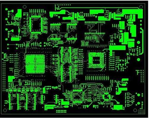
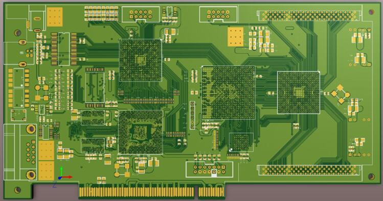
Fundamentally speaking, electromagnetic compatibility is tested and verified against existing models in the test chamber. These tests are not only expensive but also time-consuming. There are many ways to use early software simulation in the design process to reduce the cost of testing. However, EMC is a complex subject, and it is very difficult to achieve complete 3D simulation of complex circuit boards at present. Because of these difficulties, experts can only focus on the simulation of key areas of the circuit board, such as power and grounding systems or individual critical networks, to determine the causes of electromagnetic field radiation (emission) and radiation (sensitivity). The knowledge gained in these analyses will be applied to the design principles of PCB circuit designers.
In the newly developed simulation software package, users can see the complete wiring design from the most popular PCB layout tools. The wiring review function checks various design principles of all board layers, networks or traces. The software can import the wiring data of the following wiring tool providers: Altium, Cadence, Mentor, OrCAD and Zuken. The software is jointly developed by experts from professional simulation software companies and well-known IT industry giants.

The former provides interfaces with a variety of PCB wiring tools, while the latter focuses on an expert system that has established and verified EMC/SI rules for decades. Over the years, the company's experts have studied many EMC design issues using flexible measurement technology, and finally established various effective design rules. The critical design is checked according to these rules, and the results are verified by testing. Finally, the different functions are combined to form a software tool that can identify the main sources of common electromagnetic disturbances.
This general-purpose software does not require EMC experts. It allows PCB board designers to check whether the design complies with EMC rules. Secondly, the software provides detailed descriptions and possible solutions to the EM problem to the wiring designer. The integrated browser can display the exact location of EMC violations in the design. In fact, the main purpose of developing this software package is to enable users without relevant EMC knowledge to accurately locate EMC problems earlier and easier in the design, thereby minimizing the cost of measurement and redesign.
rule-based inspection
Emission or coupling is caused by violation of certain geometric rules. For example, considering the path of current return, each signal has a preset path for the signal trace, but there are often loops in the power layer and ground layer. The loop current always chooses the path with the least resistance; at the same time, under high frequency conditions, choose the path with the lowest impedance. This new software can determine which return path is not continuous. For example, this path may be interrupted due to a separated plane. If the loop cannot follow the signal path geometrically, then the loop current will use a different path. Depending on the size of the area around the loop current, an antenna may radiate or receive interference signals, which may lead to EMC compliance failure or possible design failure. This software tool identifies whether such discontinuous copper in the power supply layer is connected by one or more capacitors for high frequencies. Those capacitors will form a path with low impedance to the loop current, thus avoiding undesirable loops.
EMC problems caused by the capacitor being too far away from the signal to connect to the fault
Another rule is to search for networks that change the signal layer and the reference plane of the loop current. If the signal trace only changes from above to below the reference plane, the resulting radiation is very small. In this case, the loop current can continue to flow in the same plane. If the signal layer and the reference plane are changed at the same time, the return path must be guaranteed. Using capacitors near vias must avoid generating unwanted paths and loop currents. This software design rule must recognize and allow changes in the layers of the porous area under the BGA, because the reflow will not pass through the capacitor but will pass through the BGA. If this principle is violated, the vias where the layer change occurs will be highlighted by the software. At higher signal frequencies, it is necessary to reduce the length of the outer layer cable, check the maximum allowable length of the cable, and the violation will be pointed out.
Another rule is to check the maximum distance from the DC blocking capacitor to the connection pin of the supply voltage. Because the effective radius of the blocking capacitor is small, it cannot exceed the allowable distance connected to the decoupling pin. Otherwise, the capacitor has no effect and can be ignored. Violations of this rule will be listed together with the distance to each capacitor. The last important rule is that the trace cannot be too close to the edge of the reference plane layer. In this case, the line impedance will change and may cause the signal to reflect at the discontinuity of the impedance.
Through this software package, you can check specific rules, guide the user through an error list, and then display the key areas of the wiring. Changing the position of components in the early stages of the design phase can create a wiring path that prevents electromagnetic compatibility problems, eliminating the need for additional shielding or filters, thereby saving valuable circuit board space and component costs.
in conclusion
As the circuit board design becomes more and more complex, and the electromagnetic compatibility specification develops more and more stringent, it is necessary to seek a solution at the early stage of the design phase. The software simulation package, especially when it is used together with the effective interface of widely used wiring tools, is of great significance in the product development process.