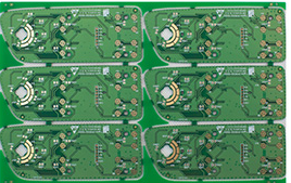
As an important part of hardware design, PCB layout is an absolutely important indicator that affects the reasonable performance of hardware circuit design. Many PCB layout engineers complete the wiring according to the limitations of hardware engineers or Pease engineers. These are usually called "pull workers." They repeated and mechanically completed a piece of PCB layout. After some time, some of them may have some experience: which should be the same length, which should be thick, which should be parallel, to ensure proper line spacing, and so on. However, they rely on the so-called experience, and many of them know they don't know what it is. I think that if we want to make a breakthrough, we must expand our knowledge.
In other words, PCB layout engineers can't let others think that they are "wire-pull workers".

First of all, you must have a certain level of circuit understanding (of course, the design ability of hardware engineers is not necessary, if possible, it is the best); second, it is necessary to let SI/PI engineers perform pi/si analysis (Of course, if possible, the ability to perform RF simulation is not required, which is the best).
With this knowledge, you can not only design a good PCB, but also get funding from hardware and SI/PI engineers, and even get advice on its circuit design from the PCB design.
Not to mention, some PCB designs summarize some principles:
One, about layout 1. Layout is a reasonable layout of circuit components.
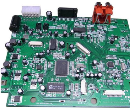
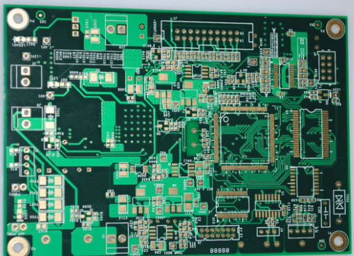
That kind of placement is reasonable. A simple principle is that the module division is very clear, that is, people use a certain circuit basis and get your PCB to see which piece is used to achieve what function.
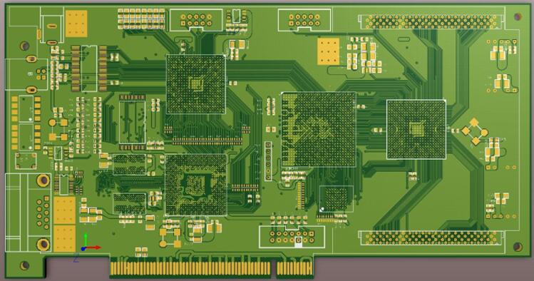
2. Specific design steps: First, form the initial PCB file according to the schematic diagram, complete the pre-layout of the PCB, determine the relative PCB layout area, and then tell the structure that the structure is based on the area we give, and then based on the overall structure design, specific constraints are given .
3. According to the constraints of the structure, complete the drawing of the board edges, positioning openings and some forbidden areas, and then complete the placement of the connectors.
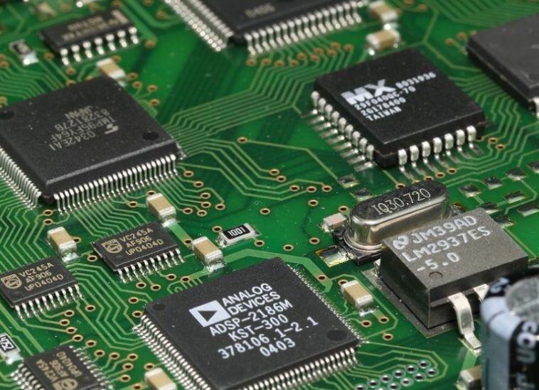
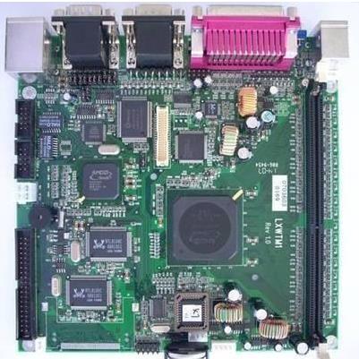
4. PCB component placement principle: Generally, the main control MCU is placed in the center of the circuit board, and then the interface circuit is placed close to the interface (such as mesh, USB, VGA, etc.), and most of the interfaces have ESD protection and filtering.
The next principle is to protect the post filter first.
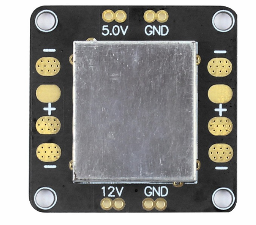
5. Then comes the power module. Generally, the main power module is placed at the power inlet (such as the system 5V), and the discrete power module (such as the module circuit power supply 2.5V) can be placed in a denser place in the same power grid according to the actual situation. 6. Some internal circuits are not introduced into the connector.
We generally follow such a basic principle: high-speed, low-speed division, analog, digital division, interference source, sensitive receptor sub-area.
7. Then for a single circuit module, follow the circuit design when designing the current. Presumably, the entire circuit layout can join and correct the great God.