The difference between a double-sided PCB circuit board and a single-sided board is that only one side of the circuit is printed with a circuit, and both sides of the circuit are printed with a double-sided circuit board. Therefore, the double-sided circuit board has a different copper sinking process except for more than one. In addition, the production process of double-sided PCB circuit boards is divided into wire method, plug hole method, mask method and pattern plating.
High-frequency electronic equipment is the development trend, especially in wireless networks, satellite communications are developing, information products are developing towards high-speed and high-frequency, and communication products are developing standardization for the ability of high-speed wireless transmission of voice, video and data.
The basic characteristics of base materials for high-frequency circuit boards are as follows:

1: Other heat resistance, chemical resistance, impact strength, peel strength, etc. must also be good.
2: Low water absorption and high water absorption will affect the dielectric constant and dielectric loss when wet.
3: The thermal expansion coefficient of the copper foil is as consistent as possible, because the inconsistency will cause the copper foil to separate in the heat and cold changes.
4: The dielectric loss (Df) must be small, which mainly affects the quality of signal transmission. The smaller the dielectric loss, the smaller the signal loss.
5: Dk must be small and stable, usually the smaller the better, the signal transmission rate is inversely proportional to the square root of the material's dielectric constant, high dielectric constant is easy to soften, resulting in signal transmission delay.
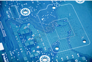
Double-sided PCB board is an important PCB board in circuit boards. There are double-sided circuit boards, metal base PCB boards, Hi-Tg heavy copper foil circuit boards, flat winding double-sided circuit boards, high-frequency PCBs, and hybrid dielectrics in the PCB market. Basic high-frequency double-sided circuit boards are suitable for a variety of high-tech industries, such as: telecommunications, power supplies, computers, industrial control, digital products, scientific and educational equipment, medical equipment, automobiles, and aerospace defense.
Circuit board preparation
Double-sided printing plates are usually made of epoxy glass coated with copper foil. It is mainly used for high-performance requirements of communication electronic equipment, advanced instruments and electronic computers.
The production process of double-sided panels is generally divided into process line method, hole plugging method, mask method and pattern electroplating an etching method, etc. The production process of pattern electroplating method is shown in the figure.
The most commonly used process for double-sided PCB proofing. At the same time, pine wood process, OSP process, gold plating process, gold and silver electroplating processes are also applicable to double-sided boards.
Tin spray technology: good appearance, silver plated pad, easy to tin plate, easy to solder, low price.
Si-gold process: stable quality, usually used in the situation of knocking IC.
The constraint management system displays the physical/spacing and high-speed rules and their status in real time according to the current state of the design, and can be applied to any stage of the design process. Each worksheet provides a spreadsheet interface that allows users to define and manage in a hierarchical manner And confirm different rules. This powerful functional application allows designers to create, edit, and evaluate constraint sets, use graphics as the topology of the graphics, and use electronic blueprints as the ideal implementation strategy. Once the constraints are submitted to the database, they can be used to drive the signal line placement and routing process. The constraint management system has been fully integrated into the PCB editor. Constraints can be confirmed in real time as the design process progresses. The result of the confirmation process will graphically indicate whether the constraints are met. Satisfactory limits are shown in green and red, with no limits, which allows designers to view the progress of the design and the impact of any design changes in the spreadsheet in a timely manner.