Application of Protel99se to Design Electronic Clock PCB Circuit
In view of the development trend of modern electronic products, the impact of PCB functions on the performance of the entire electronic product is becoming more and more obvious. Therefore, it is very important to design a circuit board that meets the process requirements and meets the normal working performance of the product.
Combining the author's many years of teaching and research experience in electronic professional courses, combined with the development of microcontrollers and circuit board design, this article will introduce in detail the design of electronic clock circuit boards for typical products developed by protel99se software for microcontrollers and notes.
1: Precautions and steps for designing circuit schematic diagrams with protel99se software

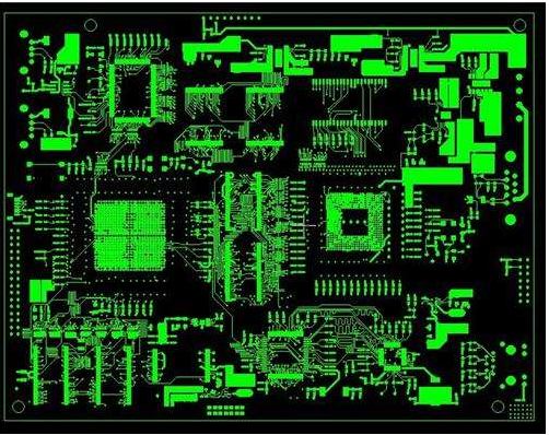
The PCB schematic diagram is the most basic basis to realize the circuit function, and the circuit schematic diagram reflects the electrical connection of various electronic components. In the design process of electronic products, the drawing of the schematic diagram is the basis for drawing the PCB. The schematic diagram is also the basis for the installation and commissioning of products by engineers and technicians. Therefore, in the process of designing and drawing the schematic diagram, the steps and process requirements of the schematic diagram must be strictly followed. In the process of drawing the schematic diagram, strictly follow the basic process requirements such as top-down, left-to-right, and signal flow. According to the functional modules of the circuit component layout, all wiring should be structured as much as possible, and the overall drawing requires the structure to be complete, beautiful and easy to read. For more complex product schematics, layered circuit PCB design ideas can be used. The structure of this circuit is clear and meets the basic requirements of schematic design. In the electronic clock schematic diagram, considering the complexity of the circuit, the overall circuit schematic diagram composed of the single-chip control circuit, time display circuit, date and temperature display circuit is adopted in the circuit board design. In the sub-circuit, in order to enhance the readability of the schematic diagram and the convenience of connection, a large number of network tags are used as the electrical connection of the device in the schematic diagram of the circuit. The overall schematic diagram of the design of the electronic clock circuit and the time display circuit schematic diagram of one of the sub-circuits.
2: Check entry for correct packaging definition and electrical rules of components
The component package is the position of the outer frame and the solder joints, and the position is indicated by the components placed on the electronic circuit board. Different components can share the same component package, and the same component can also have different packages. Usually, after completing the schematic diagram, a suitable package is defined according to the actual requirements of each component. Generally, the general standard software package library available in the software can meet the design requirements of general products. In modern printed circuit board design and development enterprises, there are generally standard packaging libraries built by the company.
The printed circuit board designer must be familiar with the packaging of common devices.
For uncertain packaging, the actual measurement and self-built packaging methods can be solved. The form of the package directly determines the mountability of the circuit board, so it must be carefully analyzed and handled carefully when defining it.
The final step in the schematic circuit board design is to perform an electrical rule check. The main problem is that the software will automatically analyze whether there are multiple network names in the same network in the circuit schematic diagram, whether there are suspended and missing input signals, and whether there are errors such as renaming of non-compliant components . Electrical rules. What needs to be emphasized here is that the inspection of electrical rules cannot replace the proof that the schematic is drawn correctly. The correctness of the schematic requires the plotter's proficient drawing skills and a high sense of responsibility.