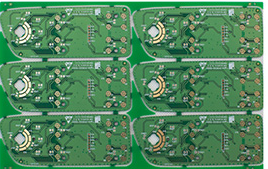
1. PCB multilayer circuit board pressing problems and solutions
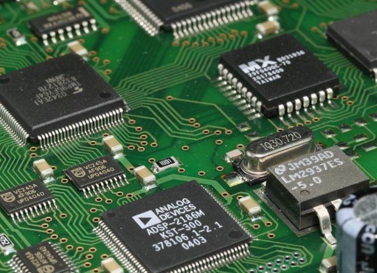
It is sufficient to make single and double panels directly to open and drill, but after drilling the PCB multilayer board, it needs to be pressed and then drilled again. Various problems may occur during the pressing process. So what are the most common problems of pressing and what are the solutions? 1. The flow direction should be scientific and reasonable: such as high voltage/low voltage, input/output, strong/weak data signal, high frequency/low frequency, etc., among them the most Reasonable flow should be linear and should not merge with each other. The principle is to eliminate mutual interference. The more appropriate flow direction is a straight line, but it is difficult to achieve. The most inappropriate flow direction is circular and isolated. If it is used exclusively for DC, the design requirements of low-voltage PCB boards may be reduced. The so-called "scientific rationality" is only relative. 2. Reasonable layout of power supply filter/decoupling capacitor: PCB layout is very important to the appearance and performance of the entire circuit board. Only part of the power supply filter/decoupling capacitor is drawn in the schematic, but it is not clear where to connect it. I think these capacitors are set for switchgear or other components that require filtering/decoupling. The location of the capacitor must be Close to those components, and if you separate them far away, you will not find the effect. When we use power filters/decoupling capacitors scientifically and reasonably, the common problems of grounding points don't seem to be prominent anymore.

3. The grounding point is better: I can’t explain the importance of choosing a grounding point. I have discussed countless professionals. Generally speaking, the requirements are universal. For example, the multiple grounding wires of the forward amplifier should be combined and then connected to the main Grounding, and so on, in real life, due to various restrictions, it is difficult to achieve this completely, but we cannot ignore it, we should try our best to follow these principles, common problems are very flexible in actual situations, and different people have different The solution, if it can be expressed specifically for a specific PCB circuit board, it is very easy to understand. 4. Reasonable line selection: The line is of course very important! If possible, please try to make the line wider. The high-voltage and high-frequency cables should be smooth and without obvious chamfers. The rotation should not be 90°. The grounding line should As wide as possible, in order to solve the problem of the grounding point, a better way is to cover a large area of copper.
2. The latest circuit board copying skills and steps
What is the meaning of circuit board copy board? Circuit board copy board is also called "circuit board imitation" and "circuit board clone". Simply put, it is to clone PCB board data 1:1 by special means. Let me introduce professional circuit board copy board. How did the technicians copy the most original PCB documents through reverse thinking! 1: Put the PCB template provided by the customer on paper and record the model, parameters, secondary tube, tertiary tube location and The direction of the IC notch; 2: Remove all the components on the board, and remove the tin in the PAD hole at the same time, clean the PCB surface with alcohol, put it into the scanner to scan to get a clearer image, and lighten the top and bottom layers with water gauze paper Polish until the copper film is shiny, put it in the scanner again, start PHOTOSHOP, and scan the two layers separately in color;
3: Adjust the contrast and brightness of the canvas to make the part with copper film and the part without copper film have a strong contrast, then turn the second image into black and white, and check whether the lines are clear. If not, repeat this step. If it is clear, save the picture as black and white BMP format files TOP.BMP and BOT.BMP. If you find any problems with the graphics, you can also use PHOTOSHOP to repair and correct them. 4: Convert two BMP format files to PROTEL format files respectively, and transfer to two layers in PROTEL. For example, the positions of PAD and VIA that have passed through two layers basically coincide, indicating that the previous steps have been done well, if there is a deviation, Then repeat the third step. Therefore, PCB copying is a work that requires patience, because a small problem will affect the quality and the degree of matching after copying.5: Convert the BMP of the TOP layer to TOP.PCB, pay attention to the conversion to the SILK layer, which is the yellow layer, and then you can trace the line on the TOP layer, and place the device according to the drawing in the second step. Delete the SILK layer after drawing. Keep repeating until all the layers are drawn.6: Import TOP.PCB and BOT.PCB in PROTEL and combine them into one picture and it will be OK. 7: Use a laser printer to print the TOP LAYER and BOTTOM LAYER on the transparent film (1:1 ratio), and put the film on the PCB. In the last step, it must be thoroughly checked for errors. If If there is no problem, it means that the copy board is successful.