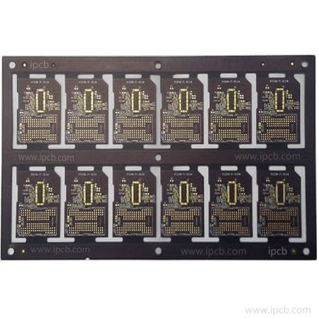

Model : 6layers 1+N+1 Mobile Phone PCB
Material : S1000-2
Layer :6Layers 1+N+1
Color :Green/White
Finished Thickness : 0.8mm
Copper Thickness : inner0.5OZ,outer1OZ
Surface Treatment :Immersion Gold+OSP
Min Trace / Space :3mil/3mil
Application :mobile phone PCB
Printed circuit board (PCB) is the support of electronic components and the provider of electrical connection of electronic components. Because it is made by electronic printing, it is called "Printed circuit board".
The design of printed circuit board is based on the circuit schematic diagram to realize the functions required by the circuit designer. Printed circuit board design mainly refers to layout design, which needs to consider various factors such as the layout of external connections, the optimal layout of internal electronic components, the optimal layout of metal wires and through holes, electromagnetic protection, thermal dissipation and other factors.
Excellent layout design can save production cost and achieve good circuit performance and heat dissipation performance. Simple layout design can be realized by hand, while complex layout design needs to be realized by computer aided design (CAD).

ipcb company's layout requirements for mobile phone PCB
1. Spacing requirements in order to ensure that the distance between components on PCB can meet the mass production capacity of SMT of our company, the distance between components (distance from side to side) ≥ 6mil.
2. Structural design requires that the layout of components should fully consider the requirements of structural design. In PCB design, we should fully communicate with structural engineers. On the premise of ensuring electrical characteristics, we should place different height and size components in different areas according to the structural design requirements.
3. Electrical characteristics require the placement of components in combination with the requirements of electrical characteristics, RF Some components cannot be placed in the baseband part, and the components in the baseband part cannot be placed in the RF part. According to the schematic diagram, components with different electrical characteristics should be distributed in different areas. In order to prevent crosstalk, each part should be isolated by shielding cover if necessary. In addition, referring to the schematic diagram, the adjacent components in the schematic diagram are also placed adjacent (such as the filtering of signal line on I / O) The wave capacitor should be placed on the pin pin of the I / O connector nearby, otherwise it can not filter. The higher the frequency, the smaller the capacitance, the closer the distance is required).
ipcb company's design specification for mobile phone PCB
1. Positioning screen printing of BGA and other devices after SMT installation of BGA packaged devices and pads, the devices that cannot be checked and need to be positioned should be added with silk screen, so that SMT can be easily checked to see if the mounting position is correct.
2. Special screen printing is designed to prevent short circuit by adding screen printing between pads which are prone to short circuit; when the shell is a metal device, if the wiring is possible to connect with metal, silk screen should be added to prevent short circuit; on directional devices, silk screen should be designed to identify the direction; the file name, version and date of PCB should be marked on the PCB with silk screen.
3. The size of screen printing requires that the width of screen printing should be no less than 7mil, so that the ipcb of PCB manufacturer can be processed clearly; the screen printing cannot be covered on the pad (PAD) of the device, otherwise the tin loading will be affected.

ipcb company's requirements for mobile phone PCB routing
Requirements for line width and distance of power line
1. The line width requirements of Vbatt power line from the input end of battery connector to pa (RF power amplifier) power pin are as follows:
When the wiring length is less than 60mm (2362mil), the line width is required to be ≥ 1.5mm (60mil); when the wiring length is greater than 60mm (2362mil), it is less than 90mm, and the line width is required to be ≥ 2mm (90mil).
In order to ensure the normal operation of PA (RF power amplifier), the total length of power lead from battery connector to PA should not be greater than 90mm (3543mil).
In addition, the line width design of high current lead is the same as that of power line.
2. The line width of other power lines is required to be 0.2mm-0.4mm (8mil-16mil) according to different current.
3. Reduce the line spacing of crosstalk between two lines. If crosstalk is easy to occur between two lines, the distance between the two lines should be greater than twice the width of the line, and the direct overlap between the upper and lower layers should be avoided (for example, there is no ground layer isolation).
4. To improve the high frequency characteristics of high-speed signal, the natural r should be used When the angle turning mode (circular arc shape) can not be fully realized, the 135 degree turning mode should be adopted, and the right angle or acute angle turning mode should be avoided; the grounding anchor of components should be directly connected to the stratum, and the nearby grounding method should be adopted if necessary, but the width of the wiring should be ensured to be no less than 0.5mm (20MIL), and long wire grounding should be avoided.
5. Routing of large devices in order to ensure the anti stripping characteristics of large devices, such as tantalum capacitors and battery connectors, tear drops or copper adhesion can be added to the leads of pads connected to these devices, and more vias connected to other layers are added.
6. The distance between the wiring and the board edge requires that the distance between the wiring and the board edge should be designed to be more than 0.4mm (16mil).
Model : 6layers 1+N+1 Mobile Phone PCB
Material : S1000-2
Layer :6Layers 1+N+1
Color :Green/White
Finished Thickness : 0.8mm
Copper Thickness : inner0.5OZ,outer1OZ
Surface Treatment :Immersion Gold+OSP
Min Trace / Space :3mil/3mil
Application :mobile phone PCB
For PCB technical problems, iPCB knowledgeable support team is here to help you with every step. You can also request PCB quotation here. Please contact E-mail sales@ipcb.com
We will respond very quickly.