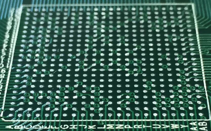
The full name of BGA is "Ball Grid Array", which means a PCB with a ball grid array structure. It is a packaging method for integrated circuits using organic carriers. PCB boards with BGA generally have more small holes, and the BGA lower through hole is usually designed as a finished hole with a diameter of 8-12mil. The BGA lower through hole needs to be plugged, the solder pad is not allowed to be inked, and the solder pad is not drilled.

BGA is a type of component that uses the solder ball array packaging method. It produces solder balls at the bottom of the packaging substrate as the interface of the circuit board, which is connected to the circuit board. BGA components are suitable for surface mount components, with a large number of pins in the circuit, higher packaging density, stronger functionality, and higher reliability. BGA's CPU is mainly used on laptops.
General rules for BGA pad design
1) The diameter of the solder pad is usually smaller than the diameter of the solder ball. To obtain reliable adhesion, it is generally reduced by 20% -25%. The larger the solder pad, the smaller the wiring space between the two pads.
2) The pad on the BGA substrate has the same diameter as the pad on the PCB.
3) The solder pad design of BGA should ensure that the template opening causes solder paste leakage of ≥ 0.08mm3, which is the minimum requirement to ensure the reliability of the solder joint.
BGA Packaging Process Principle
The main process flow of BGA packaging includes solder ball production, substrate production, chip bonding, packaging solidification, and slitting packaging.
1) Solder ball production: Using high-purity tin-lead alloy or lead-free materials to produce solder balls, forming a regular spherical pin array.
2) Substrate production: Using multi-layer printed circuit boards as substrates to achieve high-density and high-performance electrical interconnection.
3) Chip bonding: Attach the chip to the substrate and connect it to the substrate using lead-free or lead-based solder.
4) Packaging and curing: The chip is encapsulated with epoxy resin to protect it from environmental influences.
5) Split packaging: Cut the packaged chip into separate BGA packages.
BGA Packaging Techniques
1. Pad design: To ensure welding quality and reliability, pad design must follow certain guidelines. Firstly, it is necessary to ensure that the size of the solder pad matches that of the solder ball. Secondly, the influence of pad shape and layout on thermal expansion and contraction needs to be considered. Finally, attention should also be paid to the surface treatment of the solder pad to improve the reliability of welding.
2. Welding process: BGA welding usually uses reflow soldering technology. To ensure welding quality, it is necessary to control the welding temperature, time, and furnace temperature curve. In addition, attention should also be paid to the thermal stress at the moment of welding to avoid welding defects.
3. Quality inspection: After BGA packaging and welding, quality inspection is required to ensure the reliability of the connection. The commonly used detection methods include X-ray testing, acoustic emission testing, etc. X-ray inspection can visually observe the internal structure of welding points and detect welding defects. Acoustic emission testing determines the welding quality by analyzing acoustic signals.
4. Repair and maintenance: For BGA packaging with poor welding, special repair equipment can be used for re-welding. Usually, the repair process includes steps such as pad cleaning, solder ball replenishment, and chip reattachment. During the repair process, it is necessary to control the heating temperature and time to avoid damage to the chip.
5. Design and Layout: In circuit design, the layout and wiring of BGA packaging are crucial. Factors such as electrical performance, thermal performance, and mechanical strength should be fully considered. During the layout process, attention should be paid to issues such as signal integrity, power stability, and thermal management to achieve high-performance electronic systems.
Advantages and disadvantages of BGA packaging
Advantages:
1) High density: BGA packaging has a larger pin spacing, which can achieve a higher number of I/O pins and meet the requirements of high-performance integrated circuits.
2) Excellent signal transmission performance: Due to the short connection path of solder balls, BGA packaging has lower parasitic inductance and capacitance, which is conducive to high-speed signal transmission.
3) Good thermal performance: BGA-encapsulated solder balls can effectively conduct heat, helping to reduce the operating temperature of the chip.
Disadvantages:
High-demand production process: BGA packaging has high requirements for welding processes and equipment, which increases production costs.
BGA packaging is a surface mount technology characterized by the formation of a regular spherical pin array at the bottom of the package. This packaging method has advantages such as large pin spacing, good thermal performance, and superior signal transmission performance, making it widely used in high-speed and high-performance integrated circuits.