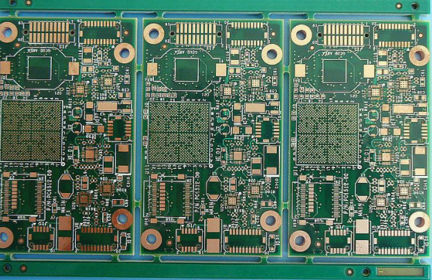
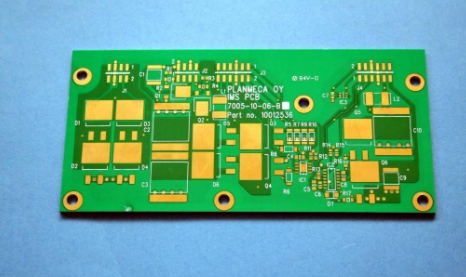
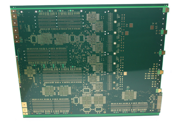
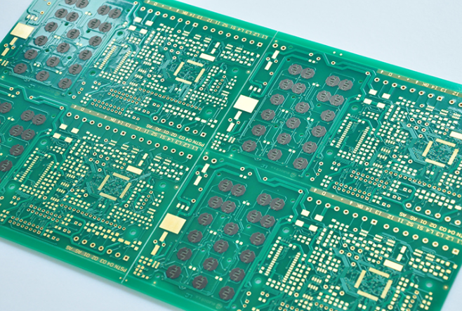
Step by step teaches you how to pick up the PCB circuit board
The first step is to get a PCB circuit board. First, record the model, parameters, and positions of all vital parts on the paper, especially the direction of the diode, the three-machine tube, and the direction of the IC gap. It is best to use a digital camera to take two photos of the location of the vital parts.
The second step is to remove all the components and remove the tin in the PAD hole. Clean the PCB with alcohol, then put it in the scanner, start POHTOSHOP, scan the silk screen surface in color, and print it out for later use.

The third step is to lightly polish the two layers of TOPLAYER and BOTTOMLAYER with water gauze paper until the copper film is shiny, put them in the scanner, start PHOTOSHOP, and scan the two layers separately in color. Note that the PCB must be placed horizontally and straight in the scanner, otherwise the scanned image cannot be used.
The fourth step is to adjust the contrast and brightness of the canvas to make the part with copper film and the part without copper film have a strong contrast, then turn the second image into black and white, and check whether the lines are clear. If not, repeat this step. If it is clear, save the picture as black and white BMP format files TOP.BMP and BOT.BMP.
The fifth step is to convert the two BMP format files into PROTEL format files, and transfer two layers in PROTEL. For example, the positions of PAD and VIA that have passed through the two layers basically coincide, indicating that the previous steps are well done. If If there is a deviation, repeat the third step.
Sixth, I will TOP. BMP is converted to TOP. PCB, pay attention to the conversion to the SILK layer, which is the yellow layer, and then you can trace the line on the TOP layer, and place the device according to the drawing in the second step. Delete the SILK layer after drawing.
The seventh step is to BOT. BMP is converted to BOT. PCB, pay attention to the conversion to the SILK layer, which is the yellow layer, and then you can trace on the BOT layer. Delete the SILK layer after drawing.
The eighth step is to TOP in PROTEL. PCB and BOT. Import the PCB and combine it into one picture and it's OK.
The ninth step, use a laser printer to print the TOPLAYER and BOTTOMLAYER on the transparent film (1:1 ratio), put the film on the PCB, and compare whether there is an error. If it is correct, you are done.
iPCB is a high-tech manufacturing enterprise focusing on the development and production of high-precision PCBs. iPCB is happy to be your business partner. Our business goal is to become the most professional prototyping PCB manufacturer in the world. Mainly focus on microwave high frequency PCB, high frequency mixed pressure, ultra-high multi-layer IC testing, from 1+ to 6+ HDI, Anylayer HDI, IC Substrate, IC test board, rigid flexible PCB, ordinary multi-layer FR4 PCB, etc. Products are widely used in industry 4.0, communications, industrial control, digital, power, computers, automobiles, medical, aerospace, instrumentation, Internet of Things and other fields.