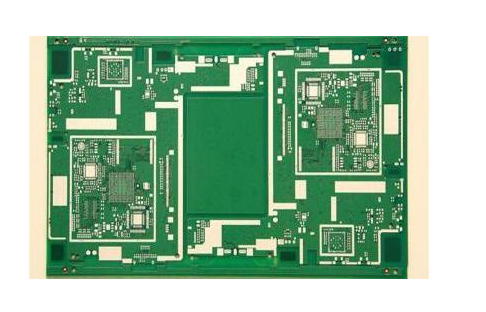
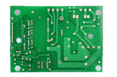
The shock of nanomaterials science to circuit board manufacturers
Everyone must have heard of nanotechnology. Nanotechnology is gradually covering our lives. So where is the mystery of nanomaterials science? What impact does it have oncircuit board manufacturers? Let us witness the impact of nanomaterials science on our circuit board manufacturers!
At present, the general development trend is centered on nanomaterials. Its high-level development is the application of nanosystem physics and its closely related nano-high-tech applications, and its popularization level development derives nanomaterial engineering and related application fields. It is not impossible that nanotechnology has caused a "turning upside down and generosity" in the field of PCB factories. Circuit board manufacturers can get irritated!

1. Reduce the dielectric constant of the circuit board substrate
The use of nano-materials to modify epoxy resins, polyimides and polyimides have been reported to reduce the dielectric constant. For example, the polyimide nano-foam material has ε<2.4.
2. Improve mechanical properties
As the particle size decreases, the surface area of the material increases, and the proportion of surface atoms in the entire material becomes larger and larger. At the same time, the surface energy and surface tension of the particles increase, and the surface atoms are more active than the atoms in the crystal lattice. Nanoparticles have many dangling bonds on the surface and are unsaturated, so they are easily combined with other atoms and stabilized, so they have great chemical activity. These high-tech fields are our circuit board manufacturers and various Large circuit board factories need to pay attention at all times.
The relationship between the specific surface of solid particles and particle size is as follows: Sw=K/(ρ*D)
Sw specific surface area m2/g K shape factor
ρ Theoretical density of particles D Average diameter of particles
Nano materials can improve the mechanical properties of epoxidized resin, at the same time can speed up the curing speed, reduce the curing temperature, combined with the development of environmentally friendly CCL, this is really a big shock to the production of our circuit board manufacturers!
3. The application of nanotechnology in the environmental protection of PCB circuit board industry
The application of nanotechnology can solve the pollution source problem of SO2, CO, NOX and other gases. For example, nano-cobalt titanate catalytic deoxidation, composite rare earth compound nano-level powder has strong redox ability, which can completely solve the pollution of CO and NOX. Circuit board manufacturers should try their best to be environmentally friendly when producing circuit boards.
With activated carbon as the carrier and nano-Zr0.5Ce0.5O2 powder as the purification catalyst of the catalytically active body, due to the presence of Zr+4/Zr+3 and Ce+4/Ce+3 on the surface, the electrons can be The transfer between valence ions has strong electron gain and loss ability and redox ability, and nanomaterials are larger than the surface, have many dangling bonds, and have strong adsorption capacity. They can reduce nitrogen oxides and oxidize CO and convert them into harmless gases. Nano-TiO2 can degrade harmful organic matter in the air.
In the past ten years, great achievements have been made in the research of nanomaterials. Various nanomaterials such as metals, alloys, ionic crystals, ceramics, oxides, nitrides, and semiconductors have been successfully prepared. New phenomena related to quantum size effect and quantum confinement and dielectric confinement effects have given us a place in the world. As far as the printed circuit board field is concerned, we are more concerned about the application results of nanomaterials science. Our circuit board manufacturers are also like this, and are very concerned about these application results in the field of nanotechnology.
Are PCB manufacturers very shocked after seeing the above nanotechnology materials? Who said that our PCB factory can't do it? Dreams are necessary, what if they are realized?