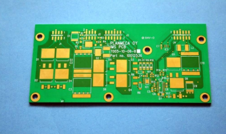
HDI board is a kind of circuit board that uses micro-blind buried via technology and tightly distributed circuits. Mainly used in high-end products, the emergence and development of HDI board have led to the emergence of light, thin, short and small electronic products.
A. The basic concept of HDI board
1. HDI: HighDensityInterconnectionTechnology high-density interconnection technology. It is a PCB multilayer board manufactured by the build-up method and micro-blind buried vias.
2. Micro-holes: In the PCB, holes with a diameter less than 6mil (150um) are called micro-holes.
3. Blind via: BlindVia, a via that connects the surface layer and the inner layer without penetrating the entire page.
4. Buried hole: BuriedViaHole, a hole buried in the inner layer, which is not visible in the finished product. It is mainly used for the conduction of the inner layer line, which can reduce the probability of signal interference and maintain the continuity of the characteristic impedance of the transmission line. Since buried vias do not occupy the surface area of the PCB, more components can be placed on the surface of the PCB.

B, the structure classification of HDI board
HDI has no fixed process, and the stacking and production process depends on the drilling requirements.
1. The composition of HDI drilling can be divided into: laser blind hole, machine drilled buried hole, machine drilled through hole.
2. According to HDI process, it can be divided into
First-order process: 1+N+1
Second-order process: 2+N+2
Third-order process: 3+N+3
Fourth-order process: 4+N+4
Three, the advantages of HDI board
1. A higher wiring density can be achieved.
2. Reduce the pad area, reduce the distance from the hole to the hole, and reduce the size of the PCB.
3. Reduce the loss of electrical signals.
High-density integrated HDI technology can make electronic products more miniaturized and meet people's needs for miniaturization of electronic products. At present, HDI is widely used in high-end electronic products such as mobile phones and digital cameras.
iPCB is a high-tech manufacturing enterprise focusing on the development and production of high-precision PCBs. iPCB is happy to be your business partner. Our business goal is to become the most professional prototyping PCB manufacturer in the world. Mainly focus on microwave high frequency PCB, high frequency mixed pressure, ultra-high multi-layer IC testing, from 1+ to 6+ HDI, Anylayer HDI, IC Substrate, IC test board, rigid flexible PCB, ordinary multi-layer FR4 PCB, etc. Products are widely used in industry 4.0, communications, industrial control, digital, power, computers, automobiles, medical, aerospace, instrumentation, Internet of Things and other fields.