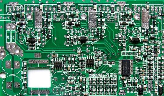
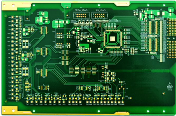
Common layout principles on PCB boards
We introduced one of the common layout principles on PCB boards-component arrangement rules. Let’s take a look at other layout principles today and make a simple reference!
According to the principle of signal layout
1). The position of each functional circuit unit is usually arranged one by one according to the signal flow, with the core element of each functional circuit as the center, and layout around it.
2). The layout of the components should facilitate the signal flow, so that the signal keeps the same direction as possible. In most cases, the signal flow is arranged from left to right or top to bottom, and the components directly connected to the input and output terminals should be placed close to the input and output connectors or connectors.
Prevent electromagnetic interference

1). For components with strong radiated electromagnetic fields and components that are more sensitive to electromagnetic induction, the distance between them should be increased or shielded, and the direction of component placement should cross the adjacent printed wires.
2). Try to avoid mixing high and low voltage devices with each other, and interleaving devices with strong and weak signals.
3). For components that generate magnetic fields, such as transformers, speakers, inductors, etc., pay attention to reducing the cutting of the printed wires by the magnetic lines of force during the layout. The magnetic field directions of adjacent components should be perpendicular to each other to reduce the coupling between each other.
4). Shield the interference source, and the shield should have a good grounding.
5). In high-frequency circuits, the influence of the distributed parameters between the components should be considered.
Common layout principles on PCB boards
Suppress thermal interference
1). For heating elements, it should be arranged in a position that is conducive to heat dissipation. If necessary, a radiator or small fan can be installed separately to reduce the temperature and reduce the impact on neighboring elements.
2). Some components such as integrated blocks with high power consumption, large or high-speed tubes, resistors, etc., should be arranged in places where heat is easy to dissipate, and separated from other components by a certain distance.
3). The thermal element should be close to the measured element and away from the high-temperature area, so as not to be affected by other heat-generating components and cause malfunction.
4). When components are placed on both sides, heating components are generally not placed on the bottom layer.
Suppress thermal interference
Layout of adjustable components
For the layout of adjustable components such as potentiometers, variable capacitors, adjustable inductance coils or micro switches, the structural requirements of the whole machine should be considered. If it is adjusted outside the machine, its position should be adapted to the position of the adjustment knob on the chassis panel; If it is adjusted inside the machine, it should be placed on the printed circuit board where it is adjusted.
Layout of adjustable components The remaining four common PCB layout principles are all introduced today. These little knowledge may one day in the future help you solve a little problem when you face a PCB that cannot run.
iPCB is a high-tech manufacturing enterprise focusing on the development and production of high-precision PCBs. iPCB is happy to be your business partner. Our business goal is to become the most professional prototyping PCB manufacturer in the world. Mainly focus on microwave high frequency PCB, high frequency mixed pressure, ultra-high multi-layer IC testing, from 1+ to 6+ HDI, Anylayer HDI, IC Substrate, IC test board, rigid flexible PCB, ordinary multi-layer FR4 PCB, etc. Products are widely used in industry 4.0, communications, industrial control, digital, power, computers, automobiles, medical, aerospace, instrumentation, Internet of Things and other fields.