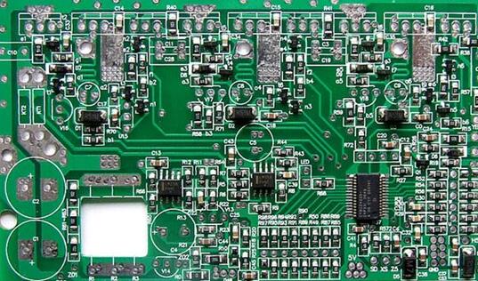
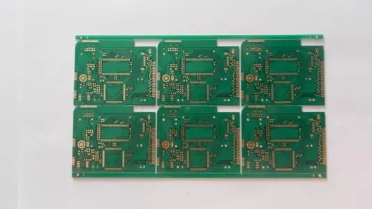
PCB board design component arrangement rules
The design and layout of the PCB board also has a lot of knowledge. At present, there are five common principles in the design of PCB boards. They are the component arrangement rule, the layout principle according to the signal direction, the principle of preventing electromagnetic interference, the principle of suppressing thermal interference, and the principle of suppressing thermal interference. Adjust the layout principle of components. Let's first introduce the arrangement rules of PCB board design components today.

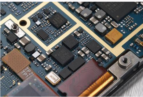
1). Under normal conditions, all components should be arranged on the same surface of the printed circuit. Only when the top components are too dense, can some devices with limited height and low heat generation, such as chip resistors and chip Capacitors, paste ICs, etc. are placed on the bottom layer.
2). On the premise of ensuring the electrical performance, the components should be placed on the grid and arranged parallel or perpendicular to each other in order to be neat and beautiful. Generally, the components are not allowed to overlap; the arrangement of the components should be compact, and the input and output components should be as far away as possible .
3). There may be a relatively high potential difference between certain components or wires, and their distance should be increased to avoid accidental short circuits due to discharge and breakdown.
4). Components with high voltage should be arranged as far as possible in places that are not easily reachable by hands during debugging.
5). The components located at the edge of the board should be at least 2 board thickness away from the edge of the board.
6). Components should be evenly distributed and densely distributed on the entire board.
This is the arrangement rules of the components on the PCB board design layout. It can be clearly seen that the arrangement of the components on the PCB board is not arbitrary. In many exhibitions, PCB boards of various shapes are passed through It is specially adjusted by technicians, otherwise the circuit board will not work. Therefore, you must be very careful when designing PCB circuits, and you must not blindly pursue novelty and uniqueness.
iPCB is a high-tech manufacturing enterprise focusing on the development and production of high-precision PCBs. iPCB is happy to be your business partner. Our business goal is to become the most professional prototyping PCB manufacturer in the world. Mainly focus on microwave high frequency PCB, high frequency mixed pressure, ultra-high multi-layer IC testing, from 1+ to 6+ HDI, Anylayer HDI, IC Substrate, IC test board, rigid flexible PCB, ordinary multi-layer FR4 PCB, etc. Products are widely used in industry 4.0, communications, industrial control, digital, power, computers, automobiles, medical, aerospace, instrumentation, Internet of Things and other fields.