What are the principles of PCB board design and layout?
In the PCB board design, the unit of the circuit board should be analyzed and the layout design should be carried out according to the function. So, what are the principles of PCB board design and layout? Let me explain it for you in detail below:
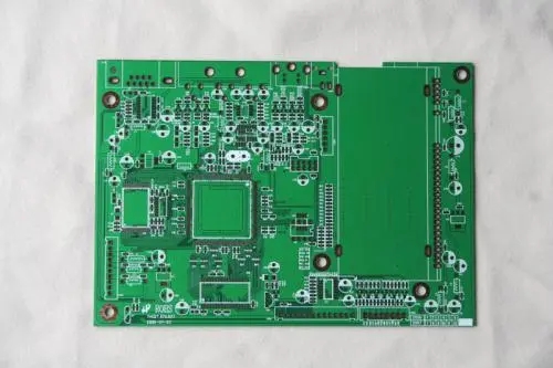
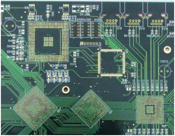
1. Under normal circumstances, all components should be placed on the same side of the circuit board. When the top components are too dense, some devices with limited height and low heat can be placed. The chip IC is placed on the lower layer.
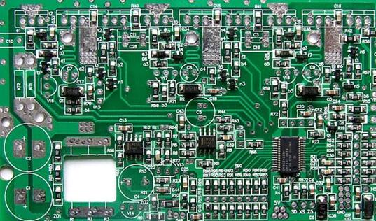
2. Under the premise of ensuring electrical performance, components should be placed on the grid and arranged in parallel or perpendicular to each other to maintain a clean and beautiful appearance. Under normal circumstances, the components are not allowed to overlap; the components are arranged compactly and evenly distributed.

3. The minimum distance between adjacent components should be less than 1MM.
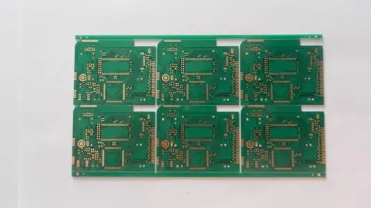
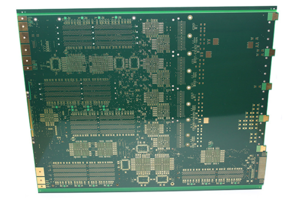
4. The edge of the board is not less than 2MM. The best shape of the board is rectangular, with an aspect ratio of 3:2 or 4:3.
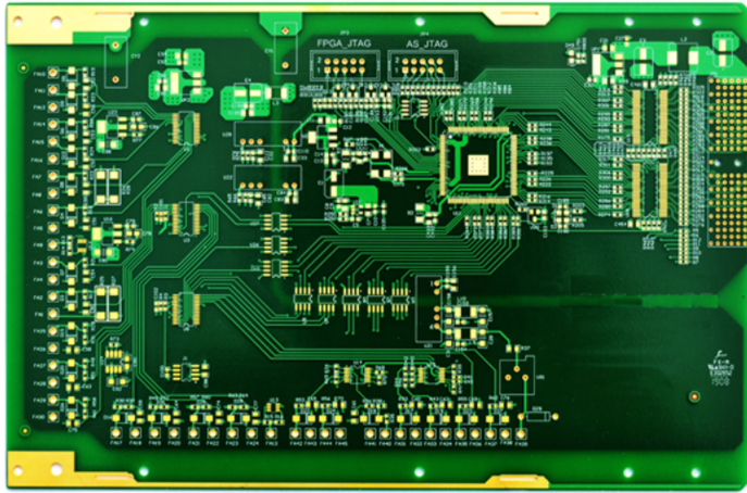
5. Arrange the position of each functional circuit unit according to the circuit flow, so that the layout is convenient for signal circulation and the signal is as consistent as possible.
6. Take the core component of each functional unit as the center and surround it. The components are uniformly and compactly arranged on the PCB to minimize the shortening of the leads and connections between the components.
7. When making the package library, pay attention to the one-to-one correspondence between the schematic pins.
8. The layout of IC decoupling capacitors should be as close as possible to the IC power supply pins, and the loop formed between the power supply and ground should be as short as possible.
9. When placing components, consider that devices using the same power supply should be placed together as much as possible to facilitate future power supply separation.
10. After the layout is completed, print out the assembly drawing for the designer to check the correctness of the device package and confirm the signal correspondence between the board, backplane and connector. After confirmation, you can start wiring.
The above is the PCB board design and layout principles explained by the editor for you. How much do you master?
iPCB is a high-tech manufacturing enterprise focusing on the development and production of high-precision PCBs. iPCB is happy to be your business partner. Our business goal is to become the most professional prototyping PCB manufacturer in the world. Mainly focus on microwave high frequency PCB, high frequency mixed pressure, ultra-high multi-layer IC testing, from 1+ to 6+ HDI, Anylayer HDI, IC Substrate, IC test board, rigid flexible PCB, ordinary multi-layer FR4 PCB, etc. Products are widely used in industry 4.0, communications, industrial control, digital, power, computers, automobiles, medical, aerospace, instrumentation, Internet of Things and other fields.