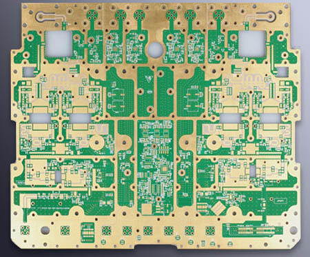
What are the PCB board design processes?
When many newcomers first enter the industry, they often don't understand the PCB board design process. Let us take a look together below:
The first stage: plan design
Engineers plan the basic modules of the circuit and draw the circuit diagram of the product according to the circuit site situation, market research or product innovation needs. This stage can be completed without altium design software. Manuscripts and other office software generally meet the requirements. The following phases need to be applied to altium design software.
The second stage: schematic design
Draw specific schematic diagrams according to the product circuit frame diagram to make the circuit system specific. The design at this stage will determine the circuit structure and PCB board design wiring scale.

The third stage: export the component network table information to the PCB board design
After drawing the schematic, the component packaging and component connection information needs to be transmitted to the PCB board design environment. The current advertising software can directly send the component network table and component packaging information to the PCB board design environment with only one command, and has the functions of seamless docking and two-way synchronization.
The fourth stage: component layout
After the component packaging is transferred to the PCB board design environment, the component layout needs to be based on the product's chassis shape, panel structure, electromagnetic compatibility specifications, reasonable requirements for electrical layout, and PCB board design laminated structure.
The fifth stage: PCB board design and wiring
After the components are arranged, the pre-pull lines generated according to the net list in the PCB board design are filled with solid lines. This filling line is the copper foil line on the finished circuit board, and the reasonableness of the circuit board wiring will directly affect the quality of the circuit board.
The sixth stage: computer-aided manufacturing process manufacturing
The electronic engineer is required to output the GERBER file for processing and manufacturing.
The above is the PCB board design process explained by the editor in detail, I hope it will be helpful to you.
iPCB is a high-tech manufacturing enterprise focusing on the development and production of high-precision PCBs. iPCB is happy to be your business partner. Our business goal is to become the most professional prototyping PCB manufacturer in the world. Mainly focus on microwave high frequency PCB, high frequency mixed pressure, ultra-high multi-layer IC testing, from 1+ to 6+ HDI, Anylayer HDI, IC Substrate, IC test board, rigid flexible PCB, ordinary multi-layer FR4 PCB, etc. Products are widely used in industry 4.0, communications, industrial control, digital, power, computers, automobiles, medical, aerospace, instrumentation, Internet of Things and other fields.