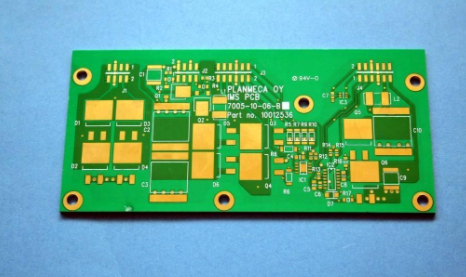
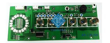
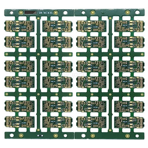
What are the important processes for ceramic substrate PCB proofing?
In PCB proofing, the ceramic substrate is relatively fragile compared to the glass fiber board, which requires relatively high process technology. There are several very important process links in the process of ceramic substrate PCB proofing. Let me share with me below:
1. Drilling
Ceramic substrates generally use laser drilling. Compared with traditional drilling technology, laser drilling technology has high accuracy, fast speed, high efficiency, large-scale batch drilling, and it is suitable for most hard, The advantages of soft materials and no loss to tools are in line with the high-density interconnection and refined development of printed circuit boards. The ceramic substrate through the laser drilling process has high bonding force between ceramic and metal, no shedding, blistering, etc., to achieve the effect of growing together, high surface flatness, roughness of 0.1μm ~ 0.3μm, laser drilling aperture It can reach 0.06mm in the range of 0.15mm-0.5mm.

2. Copper coating
Copper-clad refers to cover the area without wiring on the circuit board with copper foil and connect it to the ground wire to increase the ground wire area, reduce the loop area, reduce the voltage drop, and improve the power efficiency and anti-interference ability. In addition to reducing the impedance of the ground wire, copper coating also has the functions of reducing the cross-sectional area of the loop and enhancing the signal mirror loop. Therefore, the copper clad process plays a very critical role in the ceramic substrate PCB process. Incomplete, truncated mirror loops or incorrectly positioned copper layers often cause new interference and negatively affect the use of the circuit board.
3. Etching
The ceramic substrate also needs to be etched. The circuit pattern is pre-plated with a lead-tin anti-corrosion layer, and then the unprotected non-conductor part of the copper is etched away by chemical means to form a circuit. Etching is divided into inner layer etching and outer layer etching. The inner layer etching uses acid etching, using wet film or dry film as the resist; the outer layer etching uses alkaline etching, using tin-lead as the resist.
The above is the description of the important links of drilling, copper coating and etching in the ceramic substrate PCB proofing shared by the editor. In PCB proofing, the PCB proofing of ceramic substrates is a special process, which has high technical requirements. iPCB is a high-tech manufacturing enterprise focusing on the development and production of high-precision PCBs. iPCB is happy to be your business partner. Our business goal is to become the most professional prototyping PCB manufacturer in the world. Mainly focus on microwave high frequency PCB, high frequency mixed pressure, ultra-high multi-layer IC testing, from 1+ to 6+ HDI, Anylayer HDI, IC Substrate, IC test board, rigid flexible PCB, ordinary multi-layer FR4 PCB, etc. Products are widely used in industry 4.0, communications, industrial control, digital, power, computers, automobiles, medical, aerospace, instrumentation, Internet of Things and other fields.