PCB, IC Substrate and SLP analysis
(1) Overview of PCB industry
(1) What is PCB?
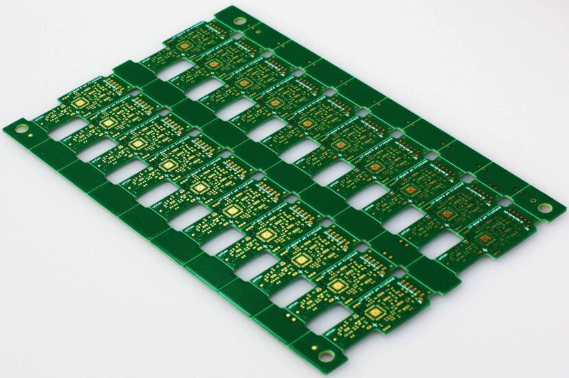
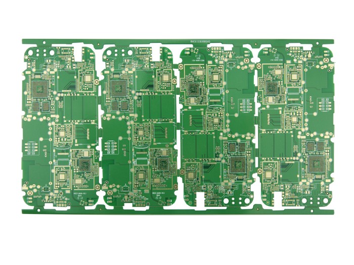
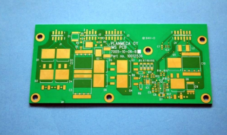
Printed Circuit Board(PCB) is a finished product with insulated substrates and conductors as materials, designed and made into printed circuits, printed components or a combination of conductive patterns according to the pre-designed circuit schematic diagram The main function of the board is to use the board-based insulating material to isolate the conductive layer of copper foil on the surface to realize the mutual connection and relay transmission between electronic components, so that the current is amplified in various electronic components along the preset line, Attenuation, modulation, decoding, coding and other functions to realize the interconnection and relay transmission between electronic components.
PCB is one of the important parts of electronic products, ranging from home appliances and mobile phones to products such as exploring the ocean and the universe. As long as there are electronic components, printed circuit boards are used for their support and interconnection. Known as the "mother of electronic products." If you compare an electronic product to a living body, then the printed circuit board is the skeleton that connects the circuit to circulate.
(2) PCB development history

As early as 1903, Mr. Albert Hanson pioneered the use of the "line" concept to be applied to the telephone switching system. It was cut into line conductors from metal foil and glued to paraffin paper, and a layer of paraffin paper was also pasted on it. The prototype of the current PCB structure. In 1925, Charles Docas printed circuit patterns on insulating substrates, and then successfully built conductors for wiring by electroplating. Until 1936, Dr. Paul Eisner invented the foil film technology. Today's "graphics transfer technology" is to follow his invention, which can be regarded as the beginning of the real PCB technology. In 1948, the United States officially recognized the invention for commercial use. In the 1950s, copper foil etching became the mainstream of PCB technology and began to be widely used. Hole metallized double-sided PCBs began mass production in the 1960s. In the 1970s, multi-layer boards developed rapidly. In the 1980s, surface mount printed boards (SMB) gradually replaced plug-in PCBs. In the 1990s, SMB developed from QFP to BGA. At the same time, PCBs for multi-chip packaging based on CSP printed boards and organic laminates developed rapidly.
Later, PCB boardsgradually developed in the direction of high density. From the early single-layer, double-layer, and multi-layer boards to HDI Microvia PCBs, HDI AnyLayer PCBs, and the current hot class carrier boards, the main feature is that the line width and line spacing are gradually reduced.
The evolution trend of PCB towards high density
(3) Packaging level and interconnection density
Semiconductors can be divided into the following levels from wafer to product packaging
• Zero-level packaging (wafer process) on-wafer circuit design and manufacturing;
• The first-level packaging (package process) bonds the chip to the lead frame or package substrate, and completes the I/O interconnection and sealing protection processes, and finally forms a packaged device. We usually say that the package is the first-level packaging;
• Second-level packaging (module or SMT process): the process of assembling components on a circuit board;
• Three-level packaging (product manufacturing process): Combine several circuit boards on a motherboard or combine several sub-systems into a complete electronic product manufacturing process.
Package level and interconnect density
The different levels of packaging actually represent different interconnect densities. The wafer usually adopts the photolithography process. At present, the 7nm process has been mass-produced, and the 5nm process has been verified and can be mass-produced next year. Here the silicon node represents the size of the gate of the integrated transistor. The line width and line spacing of the IC carrier board corresponding to the first-level package is usually less than 15μm, and the feature size of the chip is enlarged to the I/O output corresponding to the feature size of the substrate to realize the interconnection between the chip and the substrate. The PCB line width and pitch corresponding to the second-level packaging is usually greater than 40 μm, which is equivalent to enlarging the characteristic size of the substrate to the characteristic size of the PCB to realize signal interconnection.
In fact, there is a middle ground between the PCB and the IC carrier board, and this part is actually the current hot class carrier board. The demand for miniaturization of consumer electronics has led to smaller and smaller I/O outputs of the devices used. Take BGA as an example. A few years ago, the mainstream pitch of BGA was 0.6mm-0.8mm. At present, the devices used in smart phones have reached a pitch of 0.4mm and are developing towards a pitch of 0.3mm. The 0.3mm pitch design requires 30μm/30μm. At present, HDI has not met the requirements, and a higher-specification type carrier board is required. The class carrier board is the next-generation PCB rigid board, using the M-SAP process, which can shorten the line width/line spacing to 30/30μm. At present, it is widely used in high-end smart phones and some system-in-package products.
(2) PCB market analysis
(1) Cycle history of PCB industry-ups and downs
Looking back in history, since the 1980s, different electronic products such as home appliances, computers, mobile phones, and communications have emerged in an endless stream, continuously driving the continued growth and development of the electronics industry. PCB, as an important part of the electronics industry, has risen and fallen four times. After four industry cycles, each cycle is driven by innovative elements to drive the industry's rise, slow growth and decline, and then new elements appear, pushing the industry into the next cycle. .
The first stage: 1980 to 1990 was the rapid start period of the PCB industry. For the first time, the global popularity of household appliances drove the vigorous development of the PCB industry. Until 1991-1992, with the peak of the growth of traditional home appliances and the recession of the Japanese economy, the global PCB output value has fallen by about 10%.
The second stage: 1993 to 2000, is the continuous growth period of the PCB industry, mainly driven by the popularization of desktop computers and the Internet wave, new technologies HDI, FPC, etc. promote the continuous growth of the global PCB market scale, and the overall compound growth rate of the PCB industry Up to 10.57%. From 2001 to 2002, the bursting of the Internet bubble led to a global economic contraction, the demand for downstream electronic terminals slowed down, and the demand for the PCB industry was hit. Its output fell by about 25% for two consecutive years.
The third stage: From 2003 to 2008, the PCB industry maintained sustained growth (CAGR=7.73%). This is mainly due to the recovery of the global economy and the increase in demand for downstream mobile phones, notebook computers and other emerging electronic products, which has stimulated the stimulus effect of communications and consumer electronics on the PCB industry. However, the outbreak of the financial crisis in the second half of 2008 disrupted the good growth trend of the PCB industry. In 2009, the PCB industry experienced a cold winter and the total output value fell by about 15%.
The fourth stage: From 2010 to 2014, the PCB industry showed a trend of small volatility growth (CAGR=2.29%), mainly benefiting from the gradual recovery of the global economy and the driving of various downstream smart terminal products. With the upgrading of electronic products, the demand Slowing down, from 2015 to 2016, the total output value of the industry fell slightly, with a cumulative value of -5.62%.
At present, the overall development of the PCB industry is slowing down. Starting from 2017, with the emergence of new structural growth hotspots such as 5G, cloud computing, and smart cars, the PCB industry is expected to usher in new growth drivers and enter the first industry cycle development. Five stages.