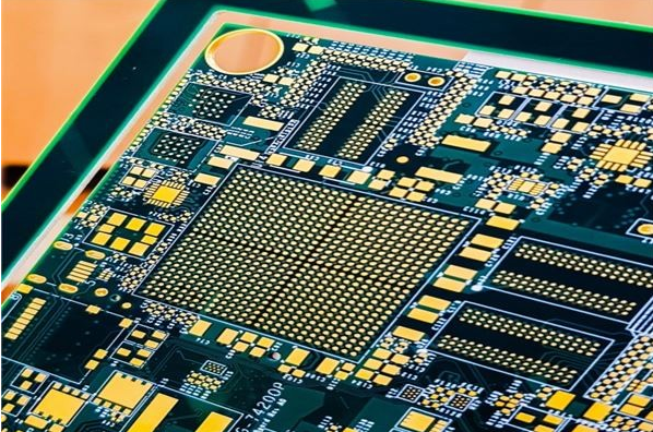
With the continuous development of semiconductor technology and deep pressure micron technology, the switching speed of IC has increased from tens of M Hz to hundreds of M Hz, and even reached several GHz. In high-speed PCB design, engineers often encounter signal integrity problems such as false trigger, damped oscillation, overshoot, undershoot and crosstalk. In this paper, the causes of their formation, calculation methods and how to solve these problems using IBIS simulation method in Allegro are discussed.
1 Signal integrity definition
Signal Integrity (SI) refers to the quality of signals on a Signal line. Poor signal integrity is not caused by a single factor, but by a combination of many factors in board level design. The causes of signal integrity
destruction include reflection, ringing, ground bounce, crosstalk, etc. With the increasing of signal frequency, signal integrity has become the focus of high speed PCB engineers.

2 the reflection
2.1 Reflection formation and calculation
Impedance discontinuities on the transmission line cause the signal to be reflected, and when the source and load impedance do not match, the load will reflect part of the voltage back to the source. Differential line transmission has solved many problems.
What is a differential signal? In plain English, the driver sends two equivalent and inverting signals, and the receiver compares the difference between the two voltages to determine whether the logical state is "0" or "1". The pair of lines that carry the differential signal are called differential lines. Differential line impedance how to calculate? All kinds of differential signal impedance is not the same, such as USB D+ D-, differential line impedance is 90ohm, 1394 difference line is 110ohm, first look at the specifications or relevant information. Now there are a lot of impedance calculation tools, such as Polar SI9000, the factors affecting differential impedance wire width, difference line spacing, dielectric dielectric constant, dielectric thickness (between the difference line and the reference surface of the dielectric thickness), generally adjust the difference line spacing and line width to control the differential impedance. When making a plate, you should also tell the manufacturer which lines to control impedance. A difference signal is a numerical representation of the difference between two physical quantities. Strictly speaking, all voltage signals are differential, since one voltage can only be relative to another voltage. In some systems, the system ground is used as a voltage reference point. When ground is used as the reference for voltage measurement, this signal planning is said to be single-ended. We use this term because signals are represented by voltage across a single conductor.
The advantage of differential signals is that, since you are controlling the 'reference' voltage, it is easy to identify small signals. In a ground-based, single-ended signal scheme, the value of the measured signal depends on the consistency of the ground-based system. The further away the source and receiver are, the greater the likelihood that their local voltage values will differ. The signal value recovered from the differential signal is largely independent of the value of 'ground', but within a certain range.
A second benefit of differential signals is that they are highly immune to external electromagnetic interference (EMI). An interference source affects each end of a differential signal pair to an almost equal degree. Since the PADSLOGIC voltage difference in PADS determines the signal value, any identical interference occurring on both conductors will be ignored. In addition to being less sensitive to interference, differential signals generate less EMI than single-ended signals.
The third advantage of differential signal is timing positioning. Since the switching change of differential signal is located at the intersection of two signals, unlike ordinary single-ended signal which depends on the judgment of high and low threshold voltage, it is less affected by process and temperature, which can reduce the timing error and is more suitable for the circuit of low amplitude signal. LVDS(Low Voltage Differential Signaling) is a popular small amplitude differential signal technology.
Differences may not consider crosstalk because their crosstalk results cancel out on acceptance. In addition, difference is to balance the line, parallel is only part of the balance.
I think the coupling of difference pairs should be required. For single line matching, although it is very mature in theory, the actual PCB line still has about 5% error (for a material, I have not done it myself). A differential line, on the other hand, can be thought of as a self-loop system, or the signals on its two signal lines are related. Loose coupling may cause interference from different sources, and for some interface circuits, the equal length of Allegro training difference pairs is an important factor in controlling line delay. So, I think the difference line should be tightly coupled.
For most high-speed PCBS today, maintaining good coupling is advantageous
But I hope you do not mistake coupling as a necessary condition for difference pairs, which sometimes limits the design ideas.
When doing high-speed design or analysis, we should not only know how most people do it, but also understand why others do it, and then understand and improve on the basis of other people's experience, and constantly exercise our creative thinIt is considered that differential signals do not need ground plane as backflow path, or that differential lines provide backflow path for each other. The cause of this misunderstanding is confused by the surface phenomenon, or the mechanism of high-speed signal transmission is not deep enough. Differential circuits are insensitive to similar ground projectiles and other noise signals that may be present in the power supply and ground plane. Ground plane offset part of the return does not represent a differential circuit is not returned as reference plane as a signal path, actually on the signal flow analysis, differential line and common single-ended walk line is consistent, the mechanism of the high frequency signal is always along the circuit of the inductance for reflow, the difference between difference line besides there are coupled to the ground, there is coupling between each other, Whichever is strongly coupled becomes the main backflow path. In PCB circuit design, the coupling between differential wiring is generally small, usually accounting for only 10~20% of the coupling degree, and most of the coupling is to the ground, so the main backflow path of differential wiring still exists in the ground plane. When the local plane discontinuity occurs, the coupling between the differential wiring will provide the main backflow path in the area without reference plane. Although the impact of the discontinuity of the reference plane on the differential wiring is not as serious as that of ordinary single-ended wiring, it will still reduce the quality of the differential signal and increase EMI, which should be avoided as far as possible. Some designers believe that the reference plane of the line of differential transmission can be removed to suppress part of the common mode signal in differential transmission, but theoretically this approach is not desirable. How to control the impedance? Without providing ground impedance loop for common-mode signal, EMI radiation is bound to be caused, which does more harm than good.
Maintaining equal spacing is considered more important than matching line length. In the actual PCB wiring, it is often unable to meet the requirements of differential design. Due to the distribution of pins, holes, and routing space and other factors, it is necessary to achieve the purpose of line length matching through appropriate winding, but the result is inevitably that part of the difference pair cannot be parallel. The important rule in PCB differential wiring design is to match the line length, other rules can be flexibly handled according to the design requirements and practical application.